ZHCSKI5D November 2019 – December 2021 SN74HCS74
PRODUCTION DATA
- 1 特性
- 2 应用
- 3 说明
- 4 Revision History
- 5 Pin Configuration and Functions
- 6 Specifications
- 7 Parameter Measurement Information
- 8 Detailed Description
- 9 Application and Implementation
- 10Power Supply Recommendations
- 11Layout
- 12Device and Documentation Support
- 13Mechanical, Packaging, and Orderable Information
封装选项
机械数据 (封装 | 引脚)
散热焊盘机械数据 (封装 | 引脚)
- BQA|14
订购信息
9.2.3 Application Curve
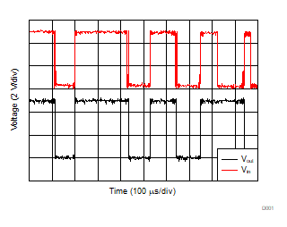
Circuit response without RC debounce
Vin := CLK input, Vout := Q output illustrates
an example of a single button press bouncing and causing the output to toggle
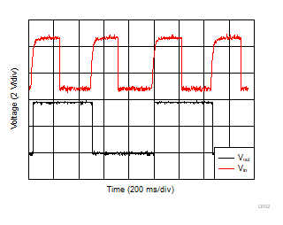
multiple times. This will cause issues in the desired application. Circuit response with RC debounce
Vin
:= CLK input, Vout := Q output illustrates 4 button presses
with an added debounce circuit, fixing the unwanted toggling and allowing for proper
toggle switch operation.
 Figure 9-2 Circuit response without RC debounce
Vin := CLK input, Vout := Q output
 Figure 9-3 Circuit response with RC debounce
Vin := CLK input, Vout := Q output