ZHCSQI9I December 2003 – March 2024 SN74AVC1T45
PRODUCTION DATA
- 1
- 1 特性
- 2 应用
- 3 说明
- 4 Pin Configuration and Functions
-
5 Specifications
- 5.1 Absolute Maximum Ratings
- 5.2 ESD Ratings
- 5.3 Recommended Operating Conditions
- 5.4 Thermal Information
- 5.5 Electrical Characteristics
- 5.6 Switching Characteristics: VCCA = 1.2V
- 5.7 Switching Characteristics: VCCA = 1.5V ± 0.1V
- 5.8 Switching Characteristics: VCCA = 1.8V ± 0.15V
- 5.9 Switching Characteristics: VCCA = 2.5V ± 0.2V
- 5.10 Switching Characteristics: VCCA = 3.3V ± 0.3V
- 5.11 Operating Characteristics
- 5.12 Typical Characteristics
- 6 Parameter Measurement Information
- 7 Detailed Description
- 8 Application and Implementation
- 9 Device and Documentation Support
- 10Revision History
- 11Mechanical, Packaging, and Orderable Information
封装选项
请参考 PDF 数据表获取器件具体的封装图。
机械数据 (封装 | 引脚)
- DBV|6
- DRL|6
- YZP|6
- DCK|6
散热焊盘机械数据 (封装 | 引脚)
- DCK|6
订购信息
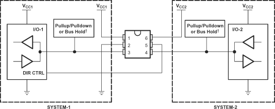
8.2.2 Bidirectional Logic Level-Shifting Application
Figure 8-3 shows the SN74AVC1T45 being used in a bidirectional logic level-shifting application. Because the SN74AVC1T45 does not have an output-enable (OE) pin, the system designer should take precautions to avoid bus contention between SYSTEM-1 and SYSTEM-2 when changing directions.
 Figure 8-3 Bidirectional Logic Level-Shifting Application
The following table provides data transmission from SYSTEM-1 to SYSTEM-2 and then from SYSTEM-2 to SYSTEM-1.
| STATE | DIR CTRL | I/O-1 | I/O-2 | DESCRIPTION |
|---|---|---|---|---|
| 1 | H | Out | In | SYSTEM-1 data to SYSTEM-2 |
| 2 | H | Hi-Z | Hi-Z | SYSTEM-2 is getting ready to send data to SYSTEM-1. I/O-1 and I/O-2 are disabled. The bus-line state depends on pullup or pulldown.(1) |
| 3 | L | Hi-Z | Hi-Z | DIR bit is flipped. I/O-1 and I/O-2 still are disabled. The bus-line state depends on pullup or pulldown.(1) |
| 4 | L | In | Out | SYSTEM-2 data to SYSTEM-1 |