ZHCSE84A October   2015  – February 2017 SN55HVD75-EP

PRODUCTION DATA.  

  1. 特性
  2. 应用范围
  3. 说明
  4. 修订历史记录
  5. Pin Configuration and Functions
  6. Specifications
    1. 6.1 Absolute Maximum Ratings
    2. 6.2 ESD Ratings
    3. 6.3 Recommended Operating Conditions
    4. 6.4 Thermal Information
    5. 6.5 Electrical Characteristics
    6. 6.6 Switching Characteristics: 20 Mbps Device, Bit Time ≥50 ns
    7. 6.7 Typical Characteristics
  7. Parameter Measurement Information
  8. Detailed Description
    1. 8.1 Overview
    2. 8.2 Functional Block Diagram
    3. 8.3 Feature Description
    4. 8.4 Device Functional Modes
  9. Application and Implementation
    1. 9.1 Application Information
    2. 9.2 Typical Application
      1. 9.2.1 Design Requirements
        1. 9.2.1.1 Data Rate and Bus Length
        2. 9.2.1.2 Stub Length
        3. 9.2.1.3 Bus Loading
        4. 9.2.1.4 Receiver Failsafe
        5. 9.2.1.5 Transient Protection
      2. 9.2.2 Detailed Design Procedure
        1. 9.2.2.1 External Transient Protection
        2. 9.2.2.2 Isolated Bus Node Design
      3. 9.2.3 Application Curve
  10. 10Power Supply Recommendations
  11. 11Layout
    1. 11.1 Layout Guidelines
    2. 11.2 Layout Example
  12. 12器件和文档支持
    1. 12.1 器件支持
      1. 12.1.1 Third-Party Products Disclaimer
    2. 12.2 接收文档更新通知
    3. 12.3 社区资源
    4. 12.4 商标
    5. 12.5 静电放电警告
    6. 12.6 Glossary
  13. 13机械、封装和可订购信息

封装选项

机械数据 (封装 | 引脚)
散热焊盘机械数据 (封装 | 引脚)
订购信息

Pin Configuration and Functions

DRB Package
8-Pin VSON
Top View
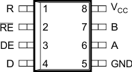
SN55HVD75-EP po_D_llse11.gif

Pin Functions

PIN TYPE DESCRIPTION
NAME NO.
A 6 Bus I/O Driver output or receiver input (complementary to B).
B 7 Bus I/O Driver output or receiver input (complementary to A).
D 4 Digital input Driver data input.
DE 3 Digital input Active-high driver enable.
GND 5 Reference potential Local device ground.
R 1 Digital output Receive data output .
RE 2 Digital input Active-low receiver enable.
VCC 8 Supply 3-V to 3.6-V supply.