ZHCSE57A September 2015 – November 2015 RF430CL331H
PRODUCTION DATA.
- 1器件概述
- 2修订历史记录
- 3Terminal Configuration and Functions
-
4Specifications
- 4.1 Absolute Maximum Ratings
- 4.2 ESD Ratings
- 4.3 Recommended Operating Conditions
- 4.4 Recommended Operating Conditions, Resonant Circuit
- 4.5 Supply Currents
- 4.6 Electrical Characteristics, Digital Inputs
- 4.7 Electrical Characteristics, Digital Outputs
- 4.8 Thermal Characteristics
- 4.9 Timing and Switching Characteristics
-
5Detailed Description
- 5.1 Overview
- 5.2 Functional Block Diagram
- 5.3 Terms and Acronyms
- 5.4 Serial Communication Interface
- 5.5 Communication Protocol
- 5.6 I2C Protocol
- 5.7 NFC Type 4B Tag Platform
- 5.8 NDEF Structure
- 5.9
Typical Operation
- 5.9.1 NDEF or Capability Container Select Procedure
- 5.9.2 NDEF or Capability Container Read Binary Procedure
- 5.9.3 NDEF or Capability Container Read Procedure (Prefetch Feature)
- 5.9.4 NDEF or Capability Container Write Procedure (Blocking)
- 5.9.5 NDEF or Capability Container Write Procedure (Nonblocking)
- 5.10 RF Command Response Timing Limits
- 5.11
Registers
- 5.11.1 General Control Register
- 5.11.2 Status Register
- 5.11.3 Interrupt Registers
- 5.11.4 CRC Registers
- 5.11.5 Communication Watchdog Register
- 5.11.6 Version Register
- 5.11.7 NDEF File Identifier Register
- 5.11.8 Host Response Register
- 5.11.9 NDEF Block Length Register
- 5.11.10 NDEF File Offset Register
- 5.11.11 Buffer Start Register
- 5.11.12 SWTX Register
- 5.11.13 Custom Status Word Response Register
- 5.12 Identification
- 6Applications, Implementation, and Layout
- 7器件和文档支持
- 8机械、封装和可订购信息
封装选项
机械数据 (封装 | 引脚)
散热焊盘机械数据 (封装 | 引脚)
订购信息
5 Detailed Description
5.1 Overview
Figure 5-1 shows the functional block diagram.
5.2 Functional Block Diagram
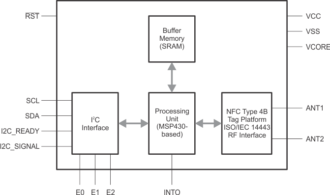 Figure 5-1 Functional Block Diagram
5.3 Terms and Acronyms
Table 5-1 describes the terms and acronyms used in this document.
Table 5-1 Term Definitions
| NAME | DESCRIPTION |
|---|---|
| PCD | Proximity coupling device, such as NFC enabled handset, NFC/RFID reader/writer devices |
| PICC | Proximity integrated circuit card, dynamic tag, RF430CL331H IC |
| NFC Type 4 command | See the NFC Forum Type 4 Tag Operation Specification (http://nfc-forum.org/) for details |
| PICC Buffer | This is a memory range (0 through 2999) that is accessible through the I2C bus, where buffer data is stored. |
| Host Controller | This is a MCU or processor connected to the PICC through the I2C bus. It responds to all the of Type 4 data requests that come from the PICC. |
| SW | Type 4 command acknowledgments, referred also as SW1 and SW2 (status word). Refer to NFC/RFID and ISO14443-B specifications for details. |
| SWTX or S(WTX) | Frame wait time extension. When the RF430CL331H cannot respond to a command that PCD sends, it must send a S(WTX) request indicating that it needs more time. The PCD then responds and the RF430CL331H has the negotiated time that it requested. |
5.4 Serial Communication Interface
The serial interface of this device is I2C. The serial interface allows a connected MCU to configure the device and write to and read from the available registers and the RAM buffer on the RF430CL331H.
5.5 Communication Protocol
The tag is programmed and controlled by writing data into and reading data from the address map shown in Table 5-2 through the I2C serial interface.
Table 5-2 User Address Map
| RANGE | ADDRESS | SIZE | DESCRIPTION |
|---|---|---|---|
| Registers | 0xFFFE | 2 B | Control register |
| 0xFFFC | 2 B | Status register | |
| 0xFFFA | 2 B | Interrupt Enable | |
| 0xFFF8 | 2 B | Interrupt Flags | |
| 0xFFF6 | 2 B | CRC Result (16-bit CCITT) | |
| 0xFFF4 | 2 B | CRC Length | |
| 0xFFF2 | 2 B | CRC Start Address | |
| 0xFFF0 | 2 B | Communication Watchdog Control register | |
| 0xFFEE | 2 B | Version | |
| 0xFFEC | 2 B | NDEF File ID register | |
| 0xFFEA | 2 B | Host Response register | |
| 0xFFE8 | 2 B | NDEF Block Length register | |
| 0xFFE6 | 2 B | NDEF File Offset register | |
| 0xFFE4 | 2 B | Buffer Start register | |
| 0xFFE2 | 2 B | Reserved | |
| 0xFFE0 | 2 B | Reserved | |
| 0xFFDE | 2 B | SWTX register | |
| 0xFFDC | 2 B | Reserved | |
| 0xFFDA | 2 B | Custom SW1 and SW2 Response | |
| Reserved | 0x4000 to 0xFFDF | Reserved | |
| 0x0BB8 to 0x3FFF | 13KB | Reserved (for example, for future extension of NDEF Memory size) | |
| Buffer | 0x0000 to 0x0BB7 | 3000 B | Buffer Memory |
NOTE
Crossing range boundaries causes writes to be ignored and reads to return undefined data.
5.6 I2C Protocol
A command is always initiated by the master by addressing the device using the specified I2C device address. The device address is a 7-bit I2C address. The upper 4 bits are hard-coded, and the lower 3 bits are programmable by the input pins E0, E1, and E2 (see Table 5-3).
Table 5-3 I2C Device Address
| BIT 6 | BIT 5 | BIT 4 | BIT 3 | BIT 2 | BIT 1 | BIT 0 |
|---|---|---|---|---|---|---|
| 0 | 0 | 1 | 1 | E2 | E1 | E0 |
| MSB | LSB |
To write data, the device is addressed using the specified I2C device address with R/W = 0, followed by the upper 8 bits of the first address to be written and the lower 8 bits of that address. Next (without a repeated START), the data to be written starting at the specified address is received. With each data byte received, the address is automatically incremented by 1. The write access is terminated by the STOP condition on the I2C bus.
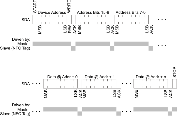 Figure 5-2 I2C Write Access
NOTE
The minimum I2C write transaction is 2 address bytes and 2 data bytes. Writes with only one 1 byte cause the data to be ignored. Avoid a transaction less than 1 data byte, as it results in an error.
To read data, the device is addressed using the specified I2C device address with R/W = 0, followed by the upper 8 bits of the first address to be read and then the lower 8 bits of that address. Next, a repeated START condition is expected with the I2C device address and R/W = 1. The device then transmit data starting at the specified address until a not acknowledge (NACK) and a STOP condition are received.
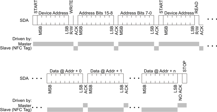 Figure 5-3 I2C Read Access
5.6.1 I2C Examples
Figure 5-4 and Figure 5-5 show examples of I2C accesses to the Control and Status registers, respectively. Comments are provided on the tags in the figures.
5.6.1.1 I2C Write
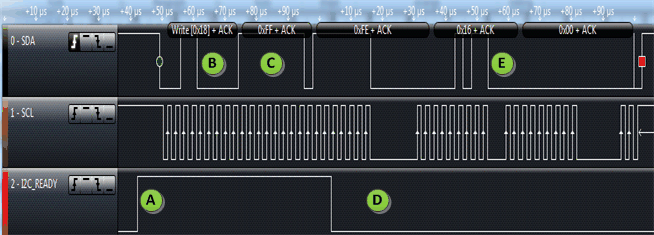 Figure 5-4 I2C Access Example: Write of the Control Register at Address 0xFFFE With 0x00, 0x16 (RF Enable = 1)
A. I2C_READY signal, by being high indicates that I2C communication can be started.
B. The device address (18h because E0 = E1 = E2 = 0) is being transmitted out.
C. Register address is 0xFFFEh (which is the Control register).
D. I2C_READY line is now low, new I2C communication should not be started.
E. The data to write is transmitted (0016h).
5.6.1.2 I2C Read
 Figure 5-5 I2C Access Example: Read of the Status Register at Address 0xFFFC, Responds With 0x00, 0x01 (Device_Ready = 1)
A. I2C_READY signal, by being high indicates that I2C communication can be started.
B. Packet has started: the device address (18h because E0 = E1 = E2 = 0) is being sent out.
C. Address FFFCh next is transmitted, which is the address of the status register.
D. An I2C restart was done and device address sent with a read selection.
E. Clock stretching is being used by the RF430CL331H when it needs more time to respond due to unfinished internal processing.
F. I2C_READY line is now low, new I2C communication should not be started.
G. RF430CL331H drives the SDA line and returns the value of the status register, which is 0001h.
H. I2C_READY signal has returned to high, indicating communication can be started. This occurs after a short period of time after a STOP condition (in square red). This brief time is necessary for the RF430CL331H to finish internal processing.
5.6.2 BIP-8 Communication Mode With I2C
The BIP-8 communication mode is enabled by setting the BIP-8 bit in the General Control register. All communication after setting this bit uses the following conventions with exactly 2 address bytes (16-bit address) and 2 data bytes (16-bit data) (see Table 5-4 and Table 5-5).
Table 5-4 Write Access
| Master | Address Bits 15 to 8 |
Address Bits 7 to 0 |
Data at Addr + 0 | Data at Addr + 1 | BIP-8 |
| Slave | N/A | N/A | N/A | N/A | N/A |
The Bit-Interleaved Parity (BIP-8) is calculated using 16-bit address and 16-bit data. If the received BIP-8 does not match with received data, no write is performed. The BIP-8 calculation does not include the I2C device address.
Table 5-5 Read Access
| Master | Address Bits 15 to 8 |
Address Bits 7 to 0 |
N/A | N/A | N/A |
| Slave | N/A | N/A | Data at Addr + 0 | Data at Addr + 1 | BIP-8 |
For read access, the Bit-Interleaved Parity (BIP-8) is calculated using the received 16-bit address and the 2 transmitted data bytes, and it is transmitted back to the master. The BIP-8 does not include the device address.
5.7 NFC Type 4B Tag Platform
This device is an NFC Forum Type 4B Tag Platform and ISO/IEC 14443B-compliant transponder that operates according to the NFC Forum Tag Type-4 specification and supports NDEF (NFC Data Exchange Format) data structure. Through the RF interface, the user can read and update the contents in the NDEF memory. The NDEF message in its entirety would only be present on the memory of the host controller. The RF430CL331H only has a portion of the NDEF message at any one time.
NOTE
This device does not have nonvolatile memory; therefore, the information stored in the NDEF memory is lost when power is removed.
This device does not support the peer-to-peer mode or the reader/writer mode. All RF communication between an NFC forum device and this device is in the passive tag mode. The device responds by load modulation and is not considered an intentional radiator.
This device is intended to be used in applications where the primary reader/writer is, for example, an NFC-enabled handset. In this case, the host application can be considered the destination device, and the cell phone or other type of mobile device is treated as the end-point device.
This device supports ISO/IEC 14443-3, ISO/IEC 14443-4, and NFC Forum commands as described in the following sections.
The device supports data rates of 106, 212, 424, and 848 kbps.
Even though all data rates up to 848 kbps are supported, the device by default reports only the capability to support 106 kbps to the PCD. To change this behavior, use the sequence described in Section 5.7.3.
The device always answers ATTRIB commands from the PCD that request higher data rates. The NFC Forum specifies for NFC-B a maximum data rate of 106 kbps. It is assumed that an NFC-compliant PCD would not request higher data rates, thus, no interoperability issues are expected.
The NFC Forum Type 4B Tag Platform and ISO/IEC 14443B command and response structure is detailed in ISO/IEC 14443-3, ISO/IEC 14443-4, and NFC Forum-TS-Digital Protocol. The applicable ISO/IEC 7816-4 commands are detailed in NFC Forum-TS-Type-4-Tag_2.0.
5.7.1 ISO/IEC 14443-3 Commands
These commands use the character, frame format, and timing that are described in ISO/IEC 14443-3, clause 7.1. The following commands are used to manage communication:
REQB and WUPB
The REQB and WUPB commands sent by the PCD are used to probe the field for PICCs of Type B. In addition, WUPB is used to wake up PICCs that are in the HALT state. The number of slots N is included in the command as a parameter to optimize the anticollision algorithm for a given application.
Slot-MARKER
After a REQB or WUPB command, the PCD may send up to (N – 1) Slot-MARKER commands to define the start of each timeslot. Slot-MARKER commands can be sent after the end of an ATQB message received by the PCD to mark the start of the next slot or earlier if no ATQB is received (no need to wait until the end of a slot, if this slot is known to be empty).
ATTRIB
The ATTRIB command sent by the PCD includes information required to select a single PICC. A PICC receiving an ATTRIB command with its identifier becomes selected and assigned to a dedicated channel. After being selected, this PICC only responds to commands defined in ISO/IEC 14443-4 that include its unique CID.
HLTB
The HLTB command is used to set a PICC in HALT state and stop responding to a REQB.
After answering to this command, the PICC ignores any commands except the WUPB.
5.7.2 NFC Tag Type 4 Commands
Select
Selection of applications or files
Read Binary
Read data from file
Update Binary
Update (erase and write) data to file
5.7.3 Data Rate Settings
The device supports data rates of 106, 212, 424, and 848 kbps.
The device always answers ATTRIB commands from the PCD that request higher data rates. The NFC Forum specifies for NFC-B a maximum data rate of 106 kbps. It is assumed that an NFC-compliant PCD would not request higher data rates, thus, no interoperability issues are expected.
Even though all data rates up to 848 kbps are supported, the device by default reports only the capability to support 106 kbps to the PCD.
To change this behavior, follow these steps using the I2C serial interface:
- If you do not want to support all data rates up to 848 kbps, change the Data Rate Capability byte according to Table 5-7. Table 5-6 summarizes how to write the data rate, and the Data Rate Capability byte is set by the DATA 0 value in Step 3. Write Access.
- Do the steps of the selected sequence. It is important to execute this sequence (in Table 5-6) before setting the Control register.
NOTE
The General Control register (see Section 5.11.1) is set to 0 after the sequence is completed in Table 5-6.
Table 5-6 Data Rate Setting Sequence
| ACCESS TYPE | ADDRESS BITS 15 TO 8 |
ADDRESS BITS 7 TO 0 |
DATA 0 | DATA 1 |
|---|---|---|---|---|
| 1. Write Access | 0xFF | 0xE0 | 0x4E | 0x00 |
| 2. Write Access | 0xFF | 0xFE | 0x80 | 0x00 |
| 3. Write Access | 0x2A | 0xBA | 0xF7 (1) | 0x00 |
| 4. Write Access | 0x27 | 0xB8 | 0x00 | 0x00 |
| 5. Write Access | 0xFF | 0xE0 | 0x00 | 0x00 |
Table 5-7 Data Rate Capability
| DATA RATA CAPABILITY BYTE | DESCRIPTION | |||||||
|---|---|---|---|---|---|---|---|---|
| B7 | B6 | B5 | B4 | B3 | B2 | B1 | B0 | |
| 0 | 0 | 0 | 0 | 0 | 0 | 0 | 0 | PICC supports only 106 kbps in both directions (default). |
| 1 | x | x | x | 0 | x | x | x | Same data rate from PCD to PICC and from PICC to PCD compulsory |
| x | x | x | 1 | 0 | x | x | x | PICC to PCD, data rate supported is 212 kbps |
| x | x | 1 | x | 0 | x | x | x | PICC to PCD, data rate supported is 424 kbps |
| x | 1 | x | x | 0 | x | x | x | PICC to PCD, data rate supported is 848 kbps |
| x | x | x | x | 0 | x | x | 1 | PCD to PICC, data rate supported is 212 kbps |
| x | x | x | x | 0 | x | 1 | x | PCD to PICC, data rate supported is 424 kbps |
| x | x | x | x | 0 | 1 | x | x | PCD to PICC, data rate supported is 848 kbps |
5.8 NDEF Structure
The NDEF message in its entirety is not stored at any time on the PICC. The host controller writes to the buffer memory as the NFC Type 4 requests come in.
Table 5-8 shows the mandatory structure. This NDEF message would be present on the memory of the host controller. For more information, refer to the NFC Forum Type 4 Tag Operation Specification (see Section 6.2).
Table 5-8 NDEF Application Data
| NDEF Application Selectable by Name = D2760000850101h |
Capability Container Selectable by File ID = E103h |
2B - CCLen | |||
| 1B - Mapping version (1) | |||||
| 2B - MLe = 000F9h (2) | |||||
| 2B - MLc = 000F6h | |||||
| NDEF File Ctrl TLV | 1B - Tag = 04h | The NDEF file control TLV is mandatory | |||
| 1B - Len = 06h | |||||
| 6B - Val | 2B - File Identifier | ||||
| 2B - Maximum file size | |||||
| 1B - Read access | |||||
| 1B - Write access | |||||
| NDEF File Selectable by File ID = xxyyh |
2B - Len | Mandatory NDEF file | |||
| xB - Binary NDEF file content | |||||
| yB - Unused if Len < Maximum file size in File Ctrl TLV | |||||
Table 5-9 NDEF Application Data (Includes Proprietary Sections)
| NDEF Application Selectable by Name = D2_7600_0085_0101h |
Capability Container Selectable by File ID = E103h |
2B - CCLen | |||
| 1B - Mapping version (1) | |||||
| 2B -MLe = 000F9h (2) | |||||
| 2B -MLc = 000F6h (2) | |||||
| NDEF File Ctrl TLV | 1B - Tag = 04h | The NDEF file control TLV is mandatory | |||
| 1B - Len = 06h | |||||
| 6B - Val | 2B - File Identifier | ||||
| 2B - Maximum file size | |||||
| 1B - Read access | |||||
| 1B - Write access | |||||
| Proprietary File Ctrl TLV (1) | 1B - Tag = 05h | Zero or more proprietary file control TLVs | |||
| 1B - Len = 06h | |||||
| 6B - Val | 2B - File Identifier | ||||
| 2B - Maximum file size | |||||
| 1B - Read access | |||||
| 1B - Write access | |||||
| ⋮ | |||||
| Proprietary File Ctrl TLV (N) | 1B - Tag = 05h | ||||
| 1B - Len = 06h | |||||
| 6B - Val | 2B - File Identifier | ||||
| 2B - Maximum file size | |||||
| 1B - Read access | |||||
| 1B - Write access | |||||
| NDEF File Selectable by File ID = xxyyh |
2B - Len | Mandatory NDEF file | |||
| xB - Binary NDEF file content | |||||
| yB - Unused if Len < Maximum file size in File Ctrl TLV | |||||
| Proprietary File (1) Selectable by File ID = xxyyh |
2B - Len | Optional proprietary file | |||
| xB - Binary proprietary file content | |||||
| yB - Unused if Len < Maximum file size in File Ctrl TLV | |||||
| ⋮ | |||||
| Proprietary File (N) Selectable by File ID = xxyyh |
2B - Len | Optional proprietary file | |||
| xB - Binary proprietary file content | |||||
| yB - Unused if Len < Maximum file size in File Ctrl TLV | |||||
5.9 Typical Operation
Figure 5-6 shows typical operation of this device. Generally, on power up or reset, the host controller initializes this device and then enables the RF. When a PCD approaches the dynamic tag, it starts by performing the ISO14443-B anticollision sequence. This portion is handled automatically by the RF430CL331H.
Eventually the sequence reaches the NFC Type 4 level. When the PCD issues a file select, Read Binary or Update Binary commands, the RF430CL331H interrupts the host controller by asserting the INT0 pin to request the necessary information or act on the information. Each type of interrupt request is detailed in the following sections.
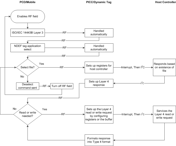 Figure 5-6 High-Level Flow
5.9.1 NDEF or Capability Container Select Procedure
This select procedure does not change between selection of the capability container or an NDEF file. These two types of selects can be differentiated by the file identifier that the RF430CL331H reports in the NDEF File Identifier register (see Section 5.11.7).
For the general flow, see Figure 5-7.
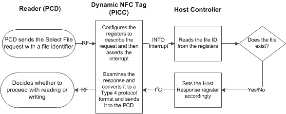 Figure 5-7 Select System Flow
The procedure:
- PCD procedure:
- Issues a Capability Container or a NDEF File Select command.
-
RF430CL331H procedure:
- Receives the RF packet.
- Sets the NDEF File Identifier register (see Section 5.11.7) using the file identifier that was included in the packet from the PCD.
- Sets up the Status register (see Section 5.11.2) and the interrupt registers (see Section 5.11.3) to describe the file select request.
- Ensure that General Type 4 request interrupt is enabled to generate the required interrupt on the INTO pin.
- Host controller procedure:
- Interrupt is received.
- Checks the source of the interrupt by reading the interrupt registers (see Section 5.11.3).
- The source of the interrupt is the General Type 4 request.
- When there is a General Type 4 request, the Status register (see Section 5.11.2) must be read and the Type 4 Command field examined to determine what Type 4 command has been received.
- The result is a File Select command.
- The NDEF File Identifier register (see Section 5.11.7) should be read.
- The host controller should, search its available files and determine if the file exists.
- The interrupt must be cleared by writing to the Interrupt Flag register (see Section 5.11.3). This step must be done before setting the Interrupt Serviced field in the Host Response register (see Section 5.11.8).
- If a specific Status Word (SW) response is necessary (generally for communicating specific error conditions) to the Select command:
- Set the Custom Status Word Response register (see Section 5.11.13) with the desired status word.
- Set the Use Custom SW Response bit in the Host Response register (see Section 5.11.8).
- To complete servicing the Select command interrupt, set the Interrupt Serviced field in the Host Response register (see Section 5.11.8).
Servicing of the Select command is complete.
-
RF430CL331H procedure:
- If the custom Status Words (SW) feature was not used:
- If the host controller indicated that the file existed, the response to the PCD is SW1 = 90h and SW2 = 00h.
- If the host controller indicated that the file did not exist, the response to the PCD is SW1 = 6Ah and SW2 = 82h.
- If the custom response feature was used, the response to the PCD is what was set in the Custom Status Word Response register (see Section 5.11.13).
- If the custom Status Words (SW) feature was not used:
5.9.2 NDEF or Capability Container Read Binary Procedure
This read procedure does not change between when the PCD reads the Capability Container or an NDEF file. These two types of reads can be differentiated by the file identifier that the RF430CL331H reports in the NDEF File Identifier register (see Section 5.11.7).
For the general flow, see Figure 5-8.
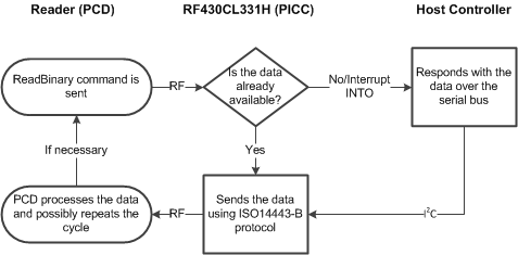 Figure 5-8 Read System Flow
The procedure:
- PCD procedure:
- Issues a Capability Container or a NDEF Read Binary command.
-
RF430CL331H procedure:
- Receives the RF packet.
- Checks its buffer and determines if all of the requested data in the Read Binary command exists already in the buffer.
- If all the data is available in the buffer then (in the case that extra data was written in a previous read request):
- No interrupt is issued to the host controller.
- The data is supplied in the response packet to the PCD automatically.
- The status word response SW1 = 90h and SW2 = 00h is appended to the packet.
- The flow returns to wait for the next Type 4 request.
- If no data or only partial data is available, then an interrupt is issued to the host controller.
- Host controller procedure:
- An interrupt is received.
- Checks the source of the interrupt by reading the interrupt registers (see Section 5.11.3).
- The source of the interrupt is the General Type 4 request.
- When there is a General Type 4 request, the Status register (see Section 5.11.2) must be read and the Type 4 Command field examined to determine what Type 4 command has been received.
- The result is a Read Binary command.
- The NDEF File Identifier register (see Section 5.11.7) may be read, but it is not necessary as it is always the file that the last Select command selected.
- Read the Buffer Start register (see Section 5.11.11) to determine where in the buffer of the RF430CL331H to begin storing the data.
- Read the NDEF File Offset register (see Section 5.11.10) to determine at which index in the NDEF or CC file to begin supplying the data to the RF430CL331H.
- Read the NDEF Block Length register (see Section 5.11.9) to determine what block length the PCD is requesting.
- Check if the request is valid:
- If it is valid, write the data into the buffer of the RF430CL331H starting at Buffer Start index for NDEF Block Length bytes.
- If it is not valid, assert the Custom Status Word option in the Host Response register (see Section 5.11.8) and write the custom word in the Custom Status Word Response register (see Section 5.11.13). Only the status word response supplied will be sent out.
- If caching is desirable, extra sequential data can be written to the RF430CL331H buffer, up to the maximum RF430CL331H buffer length (length is 3000 bytes, highest index is 2999).
- Update the NDEF Block Length register (see Section 5.11.9) with the number of bytes written into the buffer.
- The interrupt must be cleared by writing to the Interrupt Flag register. This step must be done before setting the Interrupt Serviced field in the Host Response register.
- To complete servicing the Read Binary command interrupt, set the Interrupt Serviced field in the Host Response register.
NOTE
To improve the Read Binary performance of the RF430CL331H , a caching feature may be used. After writing the requested Read Binary request data into the RF430CL331H buffer, extra sequential data may be written. If on the next Read Binary request, all of the requested data is in the buffer, the RF430CL331H automatically responds and services that request without any intervention of the host controller; that is, no interrupt is issued.
-
RF430CL331H procedure:
- Only the requested data (even if extra was supplied) is included in the response packet to the PCD. The status words are appended to the response packet per NFC Type 4 specification.
- If the command was valid, the status words are SW1 = 90h and SW2 = 00h.
- If the custom response feature was used, the response to the PCD is only what was set in the Custom Status Word Response register.
5.9.2.1 NDEF Read Command Internal Buffer Handling
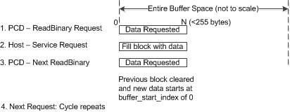 Figure 5-9 Read Buffer Flow (no extra data)
In normal read mode, when Read Prefetch functionality has not been enabled, each Read Binary request that comes in, is passed to the host controller and the internal state machine is in blocking mode until the data is sent back to the RF430CL331H . The RF430CL331H uses the same memory for each request, it is no more than the size of the read request packet length.
5.9.2.2 NDEF Read Command Internal Buffer Handling (With Caching)
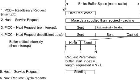 Figure 5-10 Read Buffer Flow (with caching)
- PCD requests a block of data. PICC received the requests, sets up the internal register and asserts the INTO interrupt.
- Host controller supplies the request but also adds more data on the file that is continuous with this request.
- The next PCD request is fulfilled automatically because the data that is requested is already in the buffer. The host controller is not interrupted.
- The next PCD request has insufficient data, so the data that is available is shifted to the beginning of the buffer and the unavailable data is requested.
- The full request is transmitted out.
- The cycle can repeat.
5.9.3 NDEF or Capability Container Read Procedure (Prefetch Feature)
The read prefetch feature includes the standard read procedure. However, after the requested data is written into the RF430CL331H buffer, when the RF430CL331H starts to transmit the requested data over the air, another interrupt is issued to the host controller indicating that extra data can be appended to the RF430CL331H buffer. The host controller can start adding data to the buffer while the RF430CL331H is transmitting over RF, because two tasks are happening at once, this increases the throughput of the system. For optimum operation, the host controller should cease to write extra data before the next interrupt. If the host controller does not cease to write, latency is introduced into the system, which can accumulate until requests start to time out. To determine how much is available to write the prefetch data, the time to send out the packet (that was requested) over RF can be calculated.
To enable read prefetch feature, the Read Prefetch interrupt must be enabled in the Interrupt Enable register (see Section 5.11.3).
For a general flow, see Figure 5-11.
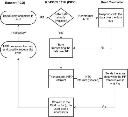 Figure 5-11 Read System Flow (Prefetch Feature)
The procedure:
- PCD procedure:
- Issues a Capability Container or a NDEF Read Binary command.
- Dynamic Tag/RF430CL331H procedure:
- Receives the RF packet.
- Checks its buffer and determines if all of the requested data in the Read Binary command exists already in the buffer.
- If all the data is available in the buffer then (in the case that extra data was written in a previous read request)
- No General Type 4 interrupt is issued to the host controller.
- The data is supplied in the response packet to the PCD automatically.
- The status word response SW1 = 90h and SW2 = 00h is appended to the packet.
- The flow now goes to Step 4e.
- If no data or only partial data is available, then a General Type 4 interrupt is issued to the host controller.
- Host controller procedure:
- Interrupt is received.
- Checks the source of the interrupt by reading the interrupt registers (see Section 5.11.3).
- The source of the interrupt is the General Type 4 request.
- When there is a General Type 4 request, the Status register (see Section 5.11.2) must be read and the Type 4 Command field examined to determine what Type 4 command has been received.
- The result is a Read Binary command.
- The NDEF File Identifier register (see Section 5.11.7) may be read, but it is not necessary as it is always the file that the last Select command selected.
- Read the Buffer Start register (see Section 5.11.11) to determine where in the buffer of the RF430CL331H to begin storing the data.
- Read the NDEF File Offset register (see Section 5.11.10) to determine at which index in the NDEF or CC file to begin supplying the data to the RF430CL331H.
- Read the NDEF Block Length register (see Section 5.11.9) to determine what block length the PCD is requesting.
- Check if the request is valid:
- If it is valid write the data into the buffer of the RF430CL331H starting at Buffer Start index for NDEF Block Length bytes.
- If it is not valid, assert the Custom Status Word option in the Host Response register (see Section 5.11.8) and write the custom word in the Custom Status Word Response register (see Section 5.11.13). Only the status word response supplied will be sent out.
- Write the requested amount of data to the buffer starting at the Buffer Start register index.
- Update the NDEF Block Length register with how much bytes were written into the buffer.
- The interrupt must be cleared by writing to the Interrupt Flag register. (This step must be done before setting the Interrupt Serviced field in the Host Response register.)
- To complete servicing the Read Binary command interrupt, set the Interrupt Serviced field in the Host Response register.
NOTE
Read caching (writing data beyond the request in a General Type 4 request interrupt) should be avoided with the prefetch feature, because caching, at least initially, creates latency because the system is waiting (blocking) for the General Type 4 request interrupt to complete. Instead, in prefetch mode, only the requested data should be supplied in the General Type 4 request interrupt. When the Extra Data interrupt occurs afterwards (in tandem with the RF transmission), only then as much as possible extra data should be written to the buffer.
- Dynamic Tag RF430CL331H procedure:
- Only the requested data (even if extra was supplied) is included in the response packet to the PCD. The status words are appended to the response packet per NFC Type 4 specification.
- If the command was valid, the status words are SW1 = 90h and SW2 = 00h.
- If the custom response feature was used, the response to the PCD is what was set in the Custom Status Word Response register.
- RF transmission starts, the Extra Data interrupt is always asserted.
- The host controller must service the Extra Data interrupt by appending to the buffer extra sequential data up until the buffer size (3000 bytes).
- Checks the source of the interrupt by reading the interrupt registers.
- The interrupt is an Extra Data interrupt.
- Read the Buffer Start register to determine where in the buffer of the RF430CL331H to begin storing the data.
- NDEF File Offset register can be read.
- Write sequential extra data to the buffer starting at the Buffer Start register index.
- The time limit of writing extra data to the buffer is until the next Read Binary command is completed to be transmitted to the RF430CL331H. After that point, latency starts to be introduced into the system as the processing of the new packet is delayed.
- Update the NDEF Block Length register with how many bytes were written into the buffer. If none, set to 0.
- The prefetch interrupt must be cleared by writing to the Interrupt Flag register.
- Set the Extra Data Send In bit in the Host Response register.
- This completes servicing of the Read Prefetch interrupt.
NOTE
When the Extra Data interrupt is enabled, the interrupt always occurs when the RF430CL331H is responding to the Read Binary request. However, this does not mean that every interrupt service can add to the RF430CL331H buffer (3000 bytes). If the Buffer Start register read indicates its index is at the end of the buffer, then no more data can be added. In this case the NDEF Block Length register should be set to 0 indicating that no data was added to the buffer. On the next Read Binary request, the valid data in the RF430CL331H buffer is shifted to the beginning to allow more room for extra data to be appended again.
5.9.3.1 NDEF Read Command With Prefetch Internal Buffer Handling
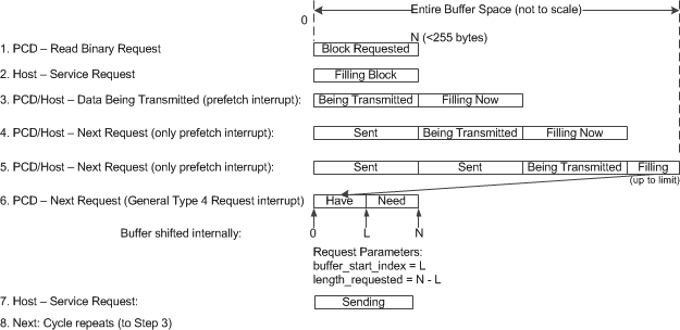 Figure 5-12 Read Buffer Flow (Prefetch Feature)
The key feature with Prefetch is that while the Read Binary is being transmitted, the next packet can be sent out by the host controller and be filling the internal RF430CL331H buffer. Each request is stored in the subsequent buffer memory until the buffer limit is reached. When the buffer limit is reached, the remaining unsent data is shifted to the beginning of the buffer and what data is needed for the next request is requested (see Step 6). This command is requested using the General Type 4 request interrupt (not with a prefetch interrupt) because it does not happen during the time when the RF430CL331H is sending data over RF.
Read buffer flow procedure (see Figure 5-12):
- PCD requests a block of data.
- PICC received the requests, sets up the internal register and asserts the INTO interrupt.
- Host services the interrupt by supplying the data. PICC transmits the data. After starting to transmit the data, PICC issues a Read Prefetch interrupt. The host supplies the extra data while the RF communication is ongoing.
- When the next Read Binary request comes, because the data is already cached, only the Prefetch interrupt is asserted.
- This time a Prefetch interrupt is asserted, but only a portion of the data can be written because the buffer space is running out.
- Because there is not enough data to service the Read Binary requests, a General Type 4 interrupt is asserted. The partial data that has been written previously is shifted to the beginning of the buffer and the only the remaining missing data is requested in the interrupt.
- The complete data is sent out. The cycle repeats (the Prefetch interrupt is issued again).
If a prefetch interrupt is issued for a file, but there is no more data to send, this interrupt can be canceled by servicing it by setting the data length sent to 0. Also if data was sent by a prefetch but it was not needed by the RF430CL331H (due to a different request by the PCD) that data is discarded and the new request handling initiated.
5.9.4 NDEF or Capability Container Write Procedure (Blocking)
This write procedure does not change between when the PCD writes the Capability Container or an NDEF file. These two types of writes can be differentiated by the file identifier that the RF430CL331H reports in the NDEF File Identifier register (see Section 5.11.7).
For a general flow, see Figure 5-13.
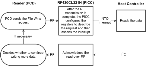 Figure 5-13 Write System Flow (Blocking)
The procedure:
- PCD procedure:
- Issues a Capability Container or a NDEF File Write (or Update Binary) command.
-
RF430CL331H procedure:
- Receives the RF Update Binary packet.
- Sets up the appropriate registers.
- Issues the General Type 4 request interrupt.
- Host controller procedure:
- Checks the source of the interrupt by reading the interrupt registers (see Section 5.11.3).
- The source of the interrupt is the General Type 4 request.
- When there is a General Type 4 request, the Status register (see Section 5.11.2) must be read and the Type 4 Command field examined to determine what Type 4 command has been received.
- The result is an Update Binary command.
- The NDEF File Identifier register (see Section 5.11.7) may be read, but it is not necessary as it is always the file that the last Select command selected.
- Read the Buffer Start register (see Section 5.11.11) to determine where in the buffer of the RF430CL331H to begin reading the stored data. Reading this register is unnecessary as it is always 0.
- Read the NDEF File Offset register (see Section 5.11.10) to determine at which index of the NDEF or CC file the current data is starting.
- Read the NDEF Block Length register (see Section 5.11.9) to determine how much data is being sent by the PCD in this packet.
- Read the data from the buffer of the RF430CL331H starting at index of 0 until the block length supplied, updating the main file on the host controller.
- If a specific Status Word (SW) response is necessary to the Update Binary command:
- Set the Custom Status Word Response register (see Section 5.11.13) with the desired status word.
- Set the Use Custom SW Response bit in the Host Response register.
- The interrupt must be cleared by writing to the Interrupt Flag register. This step must be done before setting the Interrupt Serviced field in the Host Response register.
- To complete servicing the Update Binary command interrupt, set the Interrupt Serviced field in the Host Response register.
-
RF430CL331H procedure:
- If the custom SW feature was not used, the response is status words SW1 = 90h and SW2 = 00h.
- If the custom response feature was used, the response to the PCD is what was set in the Custom Status Word Response register.
5.9.4.1 NDEF Write Command (Blocking) Internal Buffer Handling
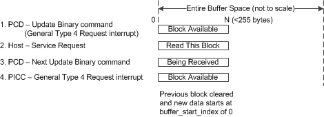 Figure 5-14 Write Buffer Flow (Blocking)
The write with blocking stores the send in data packet until it is read out by the host controller. Once it has been read out, the next write data packet is stored in the same section of memory. The cycle repeats with more Update Binary packets.
5.9.5 NDEF or Capability Container Write Procedure (Nonblocking)
This command is different from the blocking operation in that the RF430CL331H automatically responds to an Update Binary command with a success acknowledgment upon receiving the Update Binary packet.
After the acknowledgment, the PCD starts to send the next Update Binary block. The intent is to increase throughput by downloading the previous Update Binary packet while the new one is being transmitted into a separate buffer on the RF430CL331H.
Care must be taken to read out the entire packet before the new one is completely transmitted to the RF430CL331H. Otherwise, this creates latency that, if not corrected, accumulates to the point where one Update Binary packet request eventually times out.
To enable write nonblocking mode, set the Automatic ACK On Write field in the General Control register.
For a general flow, see Figure 5-15.
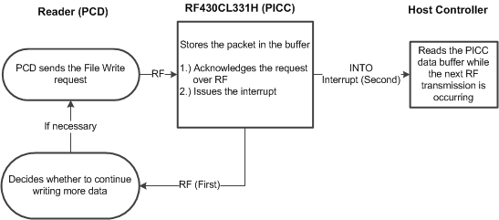 Figure 5-15 Write System Flow (Nonblocking)
- PCD procedure:
- Issues a Capability Container or a NDEF File Write (or Update Binary) command.
-
RF430CL331H procedure:
- Receives the RF Update Binary packet.
- Automatically responds with a successful acknowledgment: SW1 = 90h and SW2 = 00h.
- Sets up the appropriate registers.
- Issues the General Type 4 request interrupt.
- Waits for a new Update Binary packet to be transmitted to.
- Host controller procedure:
- Checks the source of the interrupt by reading the interrupt registers (see Section 5.11.3).
- The source of the interrupt is the General Type 4 request.
- When there is a General Type 4 request, the Status register (see Section 5.11.2) must be read and the Type 4 Command field examined to determine what Type 4 command has been received.
- The result is an Update Binary command.
- The NDEF File Identifier register (see Section 5.11.7) may be read, but it is not necessary as it is always the file that the last Select command selected.
- Read the Buffer Start register (see Section 5.11.11) to determine where in the buffer of the RF430CL331H to begin reading the stored data. Reading this register is unnecessary, as it is always 0.
- Read the NDEF File Offset register (see Section 5.11.10) to determine at which index of the NDEF or CC file the current data is starting.
- Read the NDEF Block Length register (see Section 5.11.9) to determine how much data is being sent by the PCD in this packet.
- Read the data from the buffer of the RF430CL331H, starting at the index of 0, until the block length supplied, updating the main file on the host controller.
- The interrupt must be cleared by writing to the Interrupt Flag register. This step must be done before setting the Interrupt Serviced field in the Host Response register.
- To complete servicing the Update Binary command interrupt, set the Interrupt Serviced field in the Host Response register.
5.9.5.1 NDEF Write Procedure (Nonblocking) Internal Buffer Handling
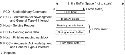 Figure 5-16 Write System Flow (Nonblocking)
The main difference in a nonblocking write operation is that when the data packet has been received from the PCD, the host controller is reading out the packet while the next one is being sent in (see Steps 3 and 4 in Figure 5-16). Data is received into a temporary buffer and when the last packet has been read out, the data in the temporary buffer is copied into the standard buffer so the data can be accessed by the host controller.
5.10 RF Command Response Timing Limits
Meeting specification timing is an important part of designing a stable and reliable system. There are various timing parameters that must be considered in this system, and one of the most important is the RF command response time.
The RF430CL331H negotiates the maximum allowable FWI timing (frame waiting time integer). This negotiated setting is the maximum of 8 (NFC Digital Protocol Section A.2, NFC-B Technology, FWIMAX), giving the time of approximately 77 ms. This is the time that the PCD allows to respond to any command.
The RF430CL331H implements an internal timer monitoring this FWI timing specification. The internal timer defaults to approximately 55 ms instead of 77 ms due to variations in the internal oscillator frequency. The 55 ms allows meeting the 77-ms specification across all devices reliably.
Figure 5-17 gives the command response timings. A detailed description follows.
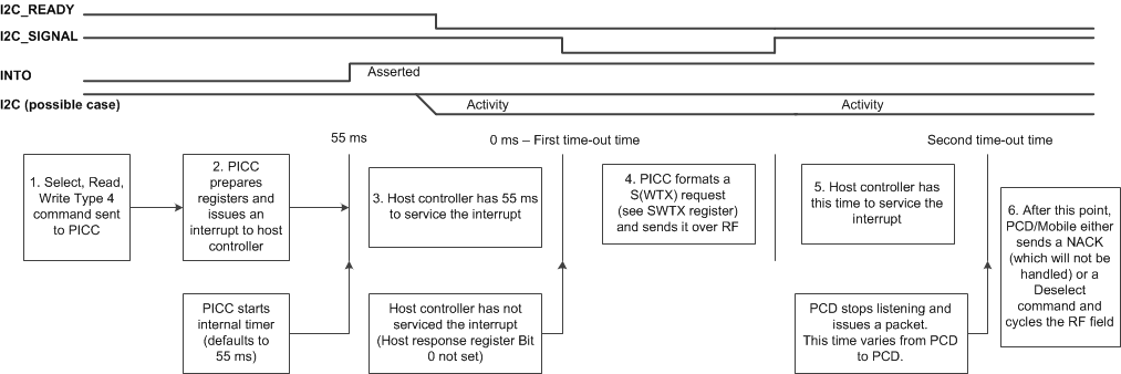 Figure 5-17 Timing Limits
- The PCD issues a Type 4 command (Select, Read Binary, or Update Binary).
- If this command needs host controller response, the RF430CL331H sets up the registers and asserts INTO.
- The RF430CL331H starts the internal initial timer of 55 ms.
- If the host controller does not respond in 55 ms, (that is, the Host Response register Interrupt Serviced Bit 0 is not set) the RF430CL331H sets the I2C_READY and I2C_SIGNAL pins to low, which. I2C_SIGNAL is a signal that is asserted when there is an active S(WTX) request ongoing. During this time the I2C communication does not have to be stopped.
- After the PICC issues the wait time extension there is another period of time in which the host controller has time to respond to the initial interrupt request.
- At this time, the PCD sends out a packet. This point should be avoided, because this will likely mean the PCD will break off communications..
- After several milliseconds, the RF430CL331H issues an S(WTX) request to the PCD.
- The WTXM field in the Frame Wait Time Extension (see Section 5.11.12) is set with the value in the SWTX register.
- Sends the Wait Time Extension request.
- Sets the I2C_SIGNAL and I2C_READY pins to high indicating that communication can continue.
- If the host controller does not service the interrupt in a certain period of time (the internal timer expires, but this does not produce an effect), the PCD issues a R(NACK) command. This and any other command are not handled by the RF430CL331H; there is no response, because the RF430CL331H command buffer still has the previous command that it has not serviced. Thus, the command must be serviced after the first S(WTX) request.
- If the PCD issues a command after the first S(WTX) command, it is likely to not be serviced, and this typically results in a Deselect command with a field reset. The communication must be restarted.
5.11 Registers
NOTE
All 16-bit registers are in little-endian format: the least significant byte with bits 7-0 is at the lowest address (this address is always even). The most significant byte with bits 15-8 is at the highest address (this address is always odd).
5.11.1 General Control Register
Table 5-10 General Control Register
| ADDRESS | 15 | 14 | 13 | 12 | 11 | 10 | 9 | 8 |
| 0xFFFF | Reserved | Automatic ACK On Write | ||||||
| ADDRESS | 7 | 6 | 5 | 4 | 3 | 2 | 1 | 0 |
| 0xFFFE | Reserved | Standby Enable | BIP-8 | INTO Drive | INTO High | Enable INT | Enable RF | SW-Reset |
Table 5-11 General Control Register Description
| BIT | FIELD | TYPE | RESET | DESCRIPTION |
|---|---|---|---|---|
| 15-9 | Reserved | R | 0 | Reserved for future use. Write with 0. |
| 8 | Automatic ACK On Write | R/W | 0 | Enabling this bit causes an automatic acknowledgment to be sent when an Update Binary command is received. The buffer must be read out immediately (possibly while a new Update Binary command is being received over RF). 0b = Manual acknowledgment of Update Binary command 1b = Automatic acknowledgment of Update Binary command |
| 7 | Reserved | R/W | 0 | |
| 6 | Standby Enable | R/W | 0 | Enables a low-power standby mode. The standby mode is entered if the RF interface is disabled, the communication watchdog is disabled, and no serial communication is ongoing. 0b = Standby mode disabled 1b = Standby mode enabled |
| 5 | BIP-8 | R/W | 0 | Enables BIP-8 communication mode (bit interleaved parity). If BIP-8 is enabled, a separate running tally is kept of the parity (that is, the number of ones that occur) for every bit position in the bytes included in the BIP-8 calculation. The corresponding bit position of the BIP-8 byte is set to 1 if the parity is currently odd and is set to 0 if the parity is even – resulting in an overall even parity for each bit position including the BIP-8 byte. All communication when this bit is set must follow the conventions defined in the BIP-8 communication mode sections in Section 5.6.2. 0b = BIP-8 communication mode disabled 1b = BIP-8 communication mode enabled |
| 4 | INTO Drive | R/W | 0 | Configuration of the interrupt output pin INTO 0b = Pin is Hi-Z if there is no pending interrupt. Application provides an external pullup resistor if bit 3 (INTO High) = 0. Application provides an external pull-down resistor if bit 3 (INTO High) = 1. 1b = Pin is actively driven high or low if there is no pending interrupt. It is driven high if bit 3 (INTO High) = 0. It is driven low if bit 3 (INTO High) = 1. |
| 3 | INTO High | R/W | 0 | Configuration of the interrupt output pin INTO 0b = Interrupts are signaled with an active low 1b = Interrupts are signaled with an active high |
| 2 | Enable INT | R/W | 0 | Global interrupt output enable 0b = Interrupt output disabled. The INTO pin is Hi-Z. 1b = Interrupt output enabled. The INTO pin signals any enabled interrupt according to the INTO High and INTO Drive bits. |
| 1 | Enable RF | R/W | 0 | Global enable of RF interface. This bit must be set before the PICC can respond to any RF commands. 0b = RF interface disabled 1b = RF interface enabled |
| 0 | SW-Reset | W | 0 | Software reset 0b = Always reads 0. 1b = Resets the device to default settings and clears memory. The serial communication is restored after tReady, and the register settings and NDEF memory must be restored afterward. |
5.11.2 Status Register
Table 5-12 Status Register
| ADDRESS | 15 | 14 | 13 | 12 | 11 | 10 | 9 | 8 |
| 0xFFFD | Reserved | |||||||
| ADDRESS | 7 | 6 | 5 | 4 | 3 | 2 | 1 | 0 |
| 0xFFFC | Reserved | Type 4 Command MSb | Type 4 Command LSb | Reserved | RF Busy | CRC Active | Device Ready | |
Table 5-13 Status Register Description
| BIT | FIELD | TYPE | RESET | DESCRIPTION |
|---|---|---|---|---|
| 15-6 | Reserved | R | 0 | Reserved for future use. Write with 0. |
| 5-4 | Type 4 Command | R | 0 | This is set after a NFC Type 4 command is received and only must be serviced if a General Type 4 request interrupt has been asserted. Bit 5 + Bit 4 00b = No Type 4 command has been received 01b = File Select Command has been received and must be serviced 10b = Read Binary command has been received and must be serviced 11b = Update Binary command has been received and must be serviced |
| 3 | Reserved | R | 0 | Reserved for future use. Write with 0. |
| 2 | RF Busy | R | 0 | 0b = No RF communication ongoing 1b = RF communication ongoing |
| 1 | CRC Active | R | 0 | 0b = No CRC calculation ongoing 1b = CRC calculation ongoing |
| 0 | Device Ready | R | 0 | 0b = Device not ready 1b = Device ready for serial communication and control |
5.11.3 Interrupt Registers
The interrupt enable register (see Table 5-14 and Table 5-15) determines which interrupt events are signaled on the external output pin INTO. Setting any bit high in this register allows the corresponding event to trigger the interrupt signal. See Table 5-18 for a description of each interrupt.
All enabled interrupt signals are ORed together, and the result is signaled on the output pin INTO.
Table 5-14 Interrupt Enable Register
| ADDRESS | 15 | 14 | 13 | 12 | 11 | 10 | 9 | 8 |
| 0xFFFB | Reserved | Read Prefetch | ||||||
| ADDRESS | 7 | 6 | 5 | 4 | 3 | 2 | 1 | 0 |
| 0xFFFA | Generic Error | RF Field Removed | General Type 4 Request | BIP-8 Error Detected | CRC Calculation Completed | Reserved | ||
Table 5-15 Interrupt Enable Register Description
| BIT | FIELD | TYPE | RESET | DESCRIPTION |
|---|---|---|---|---|
| 15-9 | Reserved | R | 0 | Reserved for future use. Write with 0. |
| 8 | Read Prefetch | R/W | 0 | Enable for the Read Prefetch IRQ. All enabled interrupt signals are ORed together, and the result is signaled on the output pin INTO. 0b = IRQ disabled 1b = IRQ enabled |
| 7 | Generic Error | R/W | 0 | Enable for the Generic Error IRQ. All enabled interrupt signals are ORed together, and the result is signaled on the output pin INTO. 0b = IRQ disabled 1b = IRQ enabled |
| 6 | RF Field Removed | R/W | 0 | Enable for the RF Field Removed IRQ. All enabled interrupt signals are ORed together, and the result is signaled on the output pin INTO. 0b = IRQ disabled 1b = IRQ enabled |
| 5 | General Type 4 Request | R/W | 0 | Enable for the General Type 4 Request IRQ. All enabled interrupt signals are ORed together, and the result is signaled on the output pin INTO. 0b = IRQ disabled 1b = IRQ enabled |
| 4 | BIP-8 Error Detected | R/W | 0 | Enable for the BIP-8 Error Detected IRQ. All enabled interrupt signals are ORed together, and the result is signaled on the output pin INTO. 0b = IRQ disabled 1b = IRQ enabled |
| 3 | CRC Calculation Completed | R/W | 0 | Enable for the CRC Calculation Completed IRQ. All enabled interrupt signals are ORed together, and the result is signaled on the output pin INTO. 0b = IRQ disabled 1b = IRQ enabled |
| 2-0 | Reserved | R | 0 | Reserved for future use. Write with 0. |
The interrupt flag register (see Table 5-16 and Table 5-17) is used to report the status of any interrupts that are pending. Setting any bit high in this register acknowledges and clears the interrupt associated with the respective bit. See Table 5-18 for a description of each interrupt.
Table 5-16 Interrupt Flag Register
| ADDRESS | 15 | 14 | 13 | 12 | 11 | 10 | 9 | 8 |
| 0xFFF9 | Reserved | Read Prefetch | ||||||
| ADDRESS | 7 | 6 | 5 | 4 | 3 | 2 | 1 | 0 |
| 0xFFF8 | Generic Error | RF Field Removed | General Type 4 Request | BIP-8 Error Detected | CRC Calculation Completed | Reserved | ||
Table 5-17 Interrupt Flag Register Description
| BIT | FIELD | TYPE | RESET | DESCRIPTION |
|---|---|---|---|---|
| 15-9 | Reserved | R | 0 | Reserved for future use. Write with 0. |
| 8 | Read Prefetch | R/W | 0 | Flag pending Read Prefetch IRQ. Read Access: 0b = No pending IRQ 1b = Pending IRQ Write Access: 0b = No change 1b = Clear pending IRQ flag |
| 7 | Generic Error | R/W | 0 | Flag pending Generic Error IRQ. Read Access: 0b = No pending IRQ 1b = Pending IRQ Write Access: 0b = No change 1b = Clear pending IRQ flag |
| 6 | RF Field Removed | R/W | 0 | Flag pending RF Field Removed IRQ. Read Access: 0b = No pending IRQ 1b = Pending IRQ Write Access: 0b = No change 1b = Clear pending IRQ flag |
| 5 | General Type 4 Request | R/W | 0 | Flag pending General Type 4 Request IRQ. Read Access: 0b = No pending IRQ 1b = Pending IRQ Write Access: 0b = No change 1b = Clear pending IRQ flag |
| 4 | BIP-8 Error Detected | R/W | 0 | Flag pending BIP-8 Error Detected IRQ. Read Access: 0b = No pending IRQ 1b = Pending IRQ Write Access: 0b = No change 1b = Clear pending IRQ flag |
| 3 | CRC Calculation Completed | R/W | 0 | Flag pending CRC Calculation Completed IRQ. Read Access: 0b = No pending IRQ 1b = Pending IRQ Write Access: 0b = No change 1b = Clear pending IRQ flag |
| 2-0 | Reserved | R | 0 | Reserved for future use. Write with 0. |
Table 5-18 Interrupts
| INTERRUPT | DESCRIPTION |
|---|---|
| CRC Calculation Completed | This IRQ occurs when a CRC calculation that is triggered by writing into the CRC registers is completed and the result can be read from the CRC result register (see Section 5.11.4). |
| BIP-8 Error Detected | This IRQ occurs when a BIP-8 error is detected (only if the BIP-8 communication mode is enabled). |
| General Type 4 Request | This IRQ occurs if a NFC Type 4 command has been received (Select, Read Binary, Update Binary) and requires the service of the host controller. |
| RF Field Removed | This IRQ occurs when at least NDEF Tag Application Select command has been received and after that the RF field is removed. |
| Generic Error | This IRQ occurs for any error that makes the device unreliable or nonoperational. |
| Read Prefetch | This IRQ occurs immediately after Read Binary request has been serviced (automatically or manually) and the RF transmission has been started. This allows RF transmission and I2C communication to happen at the same time. |
5.11.4 CRC Registers
Writing the CRC address and the CRC length registers initiates a 16-bit CRC calculation of the specified address range. The length is always assumed to be even (16-bit aligned). Writing the length register starts the CRC calculation.
During the CRC calculation, the CRC active bit is set (= 1). When the calculation is complete, the CRC completion interrupt flag is set and the result of the CRC calculation can be read from the CRC result register. TI recommends performing a CRC calculation only when the RF interface is disabled (RF Enable = 0).
Table 5-19 CRC Result Register
| ADDRESS | 15 | 14 | 13 | 12 | 11 | 10 | 9 | 8 |
| 0xFFF7 | CRC CCITT Result (high byte) | |||||||
| ADDRESS | 7 | 6 | 5 | 4 | 3 | 2 | 1 | 0 |
| 0xFFF6 | CRC CCITT Result (low byte) | |||||||
Table 5-20 CRC Result Register Description
| BIT | FIELD | TYPE | RESET | DESCRIPTION |
|---|---|---|---|---|
| 15-0 | CRC-CCITT Result | R | 0 | CRC-CCITT Result |
Table 5-21 CRC Length Register
| ADDRESS | 15 | 14 | 13 | 12 | 11 | 10 | 9 | 8 |
| 0xFFF5 | CRC Length (high byte) | |||||||
| ADDRESS | 7 | 6 | 5 | 4 | 3 | 2 | 1 | 0 |
| 0xFFF4 | CRC Length (low byte) | |||||||
Table 5-22 CRC Length Register Description
| BIT | FIELD | TYPE | RESET | DESCRIPTION |
|---|---|---|---|---|
| 15-0 | CRC Length | RW | 0 | CRC Length. Always assumed to be even (Bit 0 = 0). Writing into high byte starts CRC calculation. |
Table 5-23 CRC Start Address Register
| ADDRESS | 15 | 14 | 13 | 12 | 11 | 10 | 9 | 8 |
| 0xFFF3 | CRC Start Address (high byte) | |||||||
| ADDRESS | 7 | 6 | 5 | 4 | 3 | 2 | 1 | 0 |
| 0xFFF2 | CRC Start Address (low byte) | |||||||
Table 5-24 CRC Start Address Register Description
| BIT | FIELD | TYPE | RESET | DESCRIPTION |
|---|---|---|---|---|
| 15-0 | CRC Start Address | RW | 0 | CRC Start Address. Defines start address within NDEF memory. This address is always assumed to be even (bit 0 = 0). |
The CRC is calculated based on the CCITT polynomial initialized with 0xFFFF.
CCITT polynomial: x16 + x12 + x5 + 1
5.11.5 Communication Watchdog Register
When the communication watchdog is enabled, it expects a write or read access within a specified period; otherwise, the watchdog resets the device. If the BIP-8 communication mode is enabled, the transfer must be valid to be accepted as a watchdog reset.
Table 5-25 Communication Watchdog Register
| ADDRESS | 15 | 14 | 13 | 12 | 11 | 10 | 9 | 8 |
| 0xFFF1 | Reserved | |||||||
| ADDRESS | 7 | 6 | 5 | 4 | 3 | 2 | 1 | 0 |
| 0xFFF0 | Reserved | Time-out Period Selection | Enable | |||||
Table 5-26 Communication Watchdog Register Description
| BIT | FIELD | TYPE | RESET | DESCRIPTION |
|---|---|---|---|---|
| 15-4 | Reserved | R | 0 | Reserved for future use. Write with 0. |
| 3-1 | Time-out Period Selection | R/W | 0 | 000b = 2 s ±30% (1)
001b = 32 s ±30% (1) 010b = 8.5 min ±30% (1) 011b to 111b = Reserved |
| 0 | Enable | R/W | 0 | 0b = Communication Watchdog disabled 1b = Communication Watchdog enabled |
5.11.6 Version Register
Provides version information about the implemented ROM code.
Table 5-27 Version Register
| ADDRESS | 15 | 14 | 13 | 12 | 11 | 10 | 9 | 8 |
| 0xFFEF | Major Version | |||||||
| ADDRESS | 7 | 6 | 5 | 4 | 3 | 2 | 1 | 0 |
| 0xFFEE | Minor Version | |||||||
Table 5-28 Version Register Description
| BIT | FIELD | TYPE | RESET | DESCRIPTION |
|---|---|---|---|---|
| 15-8 | Major Version | R | 1 | Software version |
| 7-0 | Minor Version | R | 0 | Software version |
5.11.7 NDEF File Identifier Register
This register is used by the host controller to determine which file has been selected (or also for Read Binary and Update Binary commands as needed).
Table 5-29 NDEF File Identifier Register
| ADDRESS | 15 | 14 | 13 | 12 | 11 | 10 | 9 | 8 |
| 0xFFED | File Identifier Second Byte | |||||||
| ADDRESS | 7 | 6 | 5 | 4 | 3 | 2 | 1 | 0 |
| 0xFFEC | File Identifier First Byte | |||||||
Table 5-30 NDEF File Identifier Register Description
| BIT | FIELD | TYPE | RESET | DESCRIPTION |
|---|---|---|---|---|
| 15-8 | File Identifier Second Byte | R/W | 0 | This is the file identifier. It is references the second byte of the File ID in the Select command. (For example this byte for the Capability Container would be 03h). |
| 7-0 | File Identifier First Byte | R/W | 0 | This is the file identifier. It is references the first byte of the File ID in the Select command. (For example this byte for the Capability Container would be E1h). |
5.11.8 Host Response Register
This register is used, after an interrupt is asserted by the RF430CL331H. It communicates various responses from the host controller. The actual interrupt flag clearing must happen immediately before setting the response in this register.
Table 5-31 Host Response Register
| ADDRESS | 15 | 14 | 13 | 12 | 11 | 10 | 9 | 8 |
| 0xFFEB | Reserved | Reserved | Reserved | Reserved | Reserved | Reserved | Reserved | Reserved |
| ADDRESS | 7 | 6 | 5 | 4 | 3 | 2 | 1 | 0 |
| 0xFFEA | Reserved | Reserved | Reserved | Reserved | Extra Data Sent In | Use Custom SW Response | File Exists | Interrupt Serviced |
Table 5-32 Host Response Register Description
| BIT | FIELD | TYPE | RESET | DESCRIPTION |
|---|---|---|---|---|
| 15-4 | Reserved | R/W | 0 | Reserved for future use. Write with 0. |
| 3 | Extra Data Sent In | R/W | 0 | This may only be set if the Read Prefetch interrupt has been asserted. This is possible only after a Read Binary command. This indicates to the RF430CL331H that extra data has been written to the buffer during RF data transmission to a previous Read Binary command. To enable this feature, the Extra Data Interrupt Enable must be set. This also called Prefetch on Read. 0b = No extra data has been written. 1b = Extra data has been written. Update buffer size. |
| 2 | Use Custom SW Response | R/W | 0 | This sets whether or not a custom SW (status word) should be responded to a NFC Type 4 command (Select, Read Binary, Update Binary). 0b = Default response to the PCD. 1b = Custom response to the PCD. The actual SW response is taken from the Custom SW Response Register. |
| 1 | File Exists | R/W | 0 | This is the response to the interrupt of General Type 4 Request with status of file select. 0b = File named in the NDEF File Identifier Register does not exist. 1b = File named in the NDEF File Identifier Register does exist. |
| 0 | Interrupt Serviced | R/W | 0 | Setting this bit high after an interrupt (this applies only to General Type 4 Requests IRQ) has been asserted by the RF430CL331H indicates that the interrupt has been completely serviced. The actual interrupt flag clearing must happen immediately before setting this register. 0b = The interrupt is in the process of being serviced by the host controller 1b = The interrupt has been serviced, RF430CL331H to start processing the response |
5.11.9 NDEF Block Length Register
This register indicates the block length of the Read Binary or Update Binary commands to the host controller.
Table 5-33 NDEF Block Length Register
| ADDRESS | 15 | 14 | 13 | 12 | 11 | 10 | 9 | 8 |
| 0xFFE9 | Block Length MSB | |||||||
| ADDRESS | 7 | 6 | 5 | 4 | 3 | 2 | 1 | 0 |
| 0xFFE8 | Block Length LSB | |||||||
Table 5-34 NDEF Block Length Register Description
| BIT | FIELD | TYPE | RESET | DESCRIPTION |
|---|---|---|---|---|
| 15-8 | Block Length MSB | R/W | 0 | Block length most significant byte. |
| 7-0 | Block Length LSB | R/W | 0 | Block length least significant byte. |
5.11.10 NDEF File Offset Register
This register indicates the offset of the Read Binary or Update Binary commands to the host controller.
Table 5-35 NDEF File Offset Register
| ADDRESS | 15 | 14 | 13 | 12 | 11 | 10 | 9 | 8 |
| 0xFFE7 | File Offset MSB | |||||||
| ADDRESS | 7 | 6 | 5 | 4 | 3 | 2 | 1 | 0 |
| 0xFFE6 | File Offset LSB | |||||||
Table 5-36 NDEF File Offset Register Description
| BIT | FIELD | TYPE | RESET | DESCRIPTION |
|---|---|---|---|---|
| 15-8 | File Offset MSB | R/W | 0 | File offset most significant byte. |
| 7-0 | File Offset LSB | R/W | 0 | File offset least significant byte. |
5.11.11 Buffer Start Register
This register is written after a Read Binary command by the host controller indicating the index in buffer memory where the data started to be written. On an Update Binary command, this register indicates where the RF430CL331H has started to write the packet in its buffer memory.
Table 5-37 Buffer Start Register
| ADDRESS | 15 | 14 | 13 | 12 | 11 | 10 | 9 | 8 |
| 0xFFE5 | Buffer Start MSB | |||||||
| ADDRESS | 7 | 6 | 5 | 4 | 3 | 2 | 1 | 0 |
| 0xFFE4 | Buffer Start LSB | |||||||
Table 5-38 Buffer Start Register Description
| BIT | FIELD | TYPE | RESET | DESCRIPTION |
|---|---|---|---|---|
| 15-8 | Buffer Start MSB | R/W | 0 | Buffer start most significant byte. |
| 7-0 | Buffer Start LSB | R/W | 0 | Buffer start least significant byte. |
5.11.12 SWTX Register
When a PCD issues a command, there is a time-out that is negotiated (FWI in the SENSB_RES/ATQB command). The RF430CL331H has this amount of time to respond to the PCD command. If this time-out cannot be met by RF430CL331H, the NFC protocol allows a sending a S(WTX) request (refer to Section 13.2.2 of the NFC Digital Protocol). This allows the time-out to be restarted after the PCD S(WTX) response.
When the internal state machine determines that a wait time extension is necessary, it uses this register value to populate the INF field of the S(WTX) request (refer to Table 84 of the NFC Digital Protocol). This custom setting response allows flexibility in negotiating this wait time extension.
Table 5-39 SWTX Register
| ADDRESS | 15 | 14 | 13 | 12 | 11 | 10 | 9 | 8 |
| 0xFFDF | Reserved | |||||||
| ADDRESS | 7 | 6 | 5 | 4 | 3 | 2 | 1 | 0 |
| 0xFFDE | SWTX Request | |||||||
Table 5-40 SWTX Register Description
| BIT | FIELD | TYPE | RESET | DESCRIPTION |
|---|---|---|---|---|
| 15-8 | Reserved | R/W | 0 | Reserved for future use. Write with 0. |
| 7-0 | SWTX Request | R/W | 1 | S(WTX) request byte. |
5.11.13 Custom Status Word Response Register
On a NFC Type 4 command (Select, Read Binary, Update Binary), the response contains a status word (SW). This indicates whether or not the request was successful. By default, the RF430CL331H handles the SW responses automatically with predefined values. However, if custom responses are needed, for custom error status word responses, this feature may be used.
When the Use Custom SW Response is set in the Host Response register, the RF430CL331H firmware uses the SW set here to respond to the command.
Table 5-41 Custom Status Word Response Register
| ADDRESS | 15 | 14 | 13 | 12 | 11 | 10 | 9 | 8 |
| 0xFFDB | Custom Status Word Response MSB | |||||||
| ADDRESS | 7 | 6 | 5 | 4 | 3 | 2 | 1 | 0 |
| 0xFFDA | Custom Status Word Response LSB | |||||||
Table 5-42 Custom Status Word Response Register Description
| BIT | FIELD | TYPE | RESET | DESCRIPTION |
|---|---|---|---|---|
| 15-8 | Custom Status Word Response MSB | R/W | 0 | Custom status word 1 (SW1). |
| 7-0 | Custom Status Word Response LSB | R/W | 0 | Custom status word 2 (SW2). |
5.12 Identification
5.12.1 Revision Identification
The device revision information is shown as part of the top-side marking on the device package. The device-specific errata sheet describes these markings (see Section 7.2.1).
5.12.2 Device Identification
The device type can be identified from the top-side marking on the device package. The device-specific errata sheet describes these markings (see Section 7.2.1).
5.12.3 JTAG Identification
This device does not provide JTAG-compliant boundary scan test.
5.12.4 Software Identification
The Version register (see Section 5.11.6) stores the software version number.