ZHCSF35A October 2014 – June 2016 PGA300
PRODUCTION DATA.
- 1 特性
- 2 应用
- 3 说明
- 4 修订历史记录
- 5 Pin Configuration and Functions
-
6 Specifications
- 6.1 Absolute Maximum Ratings
- 6.2 ESD Ratings
- 6.3 Recommended Operating Conditions
- 6.4 Thermal Information
- 6.5 Electrical Characteristics - Reverse Voltage Protection
- 6.6 Electrical Characteristics - Regulators
- 6.7 Electrical Characteristics - Internal Reference
- 6.8 Electrical Characteristics - Bridge Sensor Supply
- 6.9 Electrical Characteristics - Temperature Sensor Supply
- 6.10 Electrical Characteristics - Internal Temperature Sensor
- 6.11 Electrical Characteristics - P Gain (Chopper Stabilized)
- 6.12 Electrical Characteristics - P Analog-to-Digital Converter
- 6.13 Electrical Characteristics - T Gain (Chopper Stabilized)
- 6.14 Electrical Characteristics - T Analog-to-Digital Converter
- 6.15 Electrical Characteristics - One-Wire Interface
- 6.16 Electrical Characteristics - DAC Output
- 6.17 Electrical Characteristics - DAC Gain
- 6.18 Electrical Characteristics - Non-Volatile Memory
- 6.19 Electrical Characteristics - Diagnostics
- 6.20 Operating Characteristics
- 6.21 Typical Characteristics
-
7 Detailed Description
- 7.1 Overview
- 7.2 Functional Block Diagram
- 7.3
Feature Description
- 7.3.1 Reverse-Voltage Protection Block
- 7.3.2 Linear Regulators
- 7.3.3 Internal Reference
- 7.3.4 BRG+ to BRG- Supply for the Resistive Bridge
- 7.3.5 ITEMP Supply for the Temperature Sensor
- 7.3.6 Internal Temperature Sensor
- 7.3.7 P Gain
- 7.3.8 P Analog-to-Digital Converter
- 7.3.9 T Gain
- 7.3.10 T Analog-to-Digital Converter
- 7.3.11 P GAIN and T GAIN Calibration
- 7.3.12 One-Wire Interface (OWI)
- 7.3.13 DAC Output
- 7.3.14 DAC Gain
- 7.3.15 Memory
- 7.3.16 Diagnostics
- 7.3.17 Digital Compensation and Filter
- 7.3.18 Filter Coefficients
- 7.4 Device Functional Modes
- 7.5
Register Maps
- 7.5.1 Register Settings
- 7.5.2
Control and Status Registers
- 7.5.2.1 DAC_CONFIG
- 7.5.2.2 OP_STAGE_CTRL
- 7.5.2.3 BRDG_CTRL
- 7.5.2.4 P_GAIN_SELECT
- 7.5.2.5 T_GAIN_SELECT
- 7.5.2.6 TEMP_CTRL
- 7.5.2.7 TEMP_SE
- 7.5.2.8 DIAG_ENABLE
- 7.5.2.9 AFEDIAG_CFG
- 7.5.2.10 AFEDIAG_MASK
- 7.5.2.11 COMPENSATION_CONTROL
- 7.5.2.12 EEPROM_LOCK
- 7.5.2.13 EEPROM_PAGE_ADDRESS
- 7.5.2.14 EEPROM_CTRL
- 7.5.2.15 EEPROM_CRC
- 7.5.2.16 EEPROM_STATUS
- 7.5.2.17 EEPROM_CRC_STATUS
- 7.5.2.18 EEPROM_CRC_VALUE
- 8 Application and Implementation
- 9 Power Supply Recommendations
- 10Layout
- 11器件和文档支持
- 12机械、封装和可订购信息
8 Application and Implementation
NOTE
Information in the following applications sections is not part of the TI component specification, and TI does not warrant its accuracy or completeness. TI’s customers are responsible for determining suitability of components for their purposes. Customers should validate and test their design implementation to confirm system functionality.
8.1 Application Information
The PGA 300 can be used in a variety of applications to measure pressure and temperature. Depending on the application, the device can be configured in different modes as illustrated in the following sections.
8.1.1 4-mA to 20-mA Output With Internal Sense Resistor
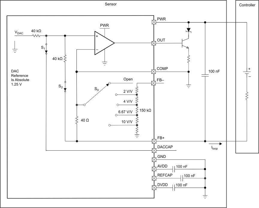
 Figure 40. 4-mA to 20-mA Output With Internal Sense Resistor Diagram
8.1.1.1 Design Requirements
There are only a few requirements to take into account when using the PGA300 device in a design:
- Do not exceed the maximum slew rate of 0.5 V/µs at the PWR pin.
- Place a 100-nF capacitor from the AVDD pin to ground, as close as possible to the AVDD pin.
- Place a 100-nF capacitor from the DVDD pin to ground, as close as possible to the DVDD pin.
- Place a capacitor between 10 nF and 1000 nF from the REFCAP pin to ground, as close as possible to the REFCAP pin.
- Place a 150-Ω resistor between the COMP pin and the emitter of the BJT for current-loop stability purposes.
- Place a 10-Ω resistor between the FB+ pin and the negative terminal of the controller for current measurement.
8.1.1.2 Detailed Design Procedure
8.1.1.2.1 Calibration Tips
8.1.1.2.1.1 Programming the EEPROM for 4-mA to 20-mA Output
The EEPROM in the PGA300 is configured by default to operate in current mode using the OP_STG_CTRL register. If not, the following sequence must be followed to change it to current mode:
- Send an OWI activation pulse to stop the digital compensation from running.
- Set OP_STAGE_CTRL to 0x80 for current mode and DAC_CONFIG EEPROM to 0x00 or 0x01 for No_Gain.
- Let the digital compensation run again to read the new EEPROM values.
8.1.1.3 Application Curve

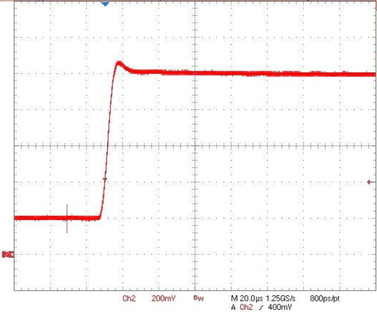
| Voltage measured between the GND pin in the PGA300 device and the negative terminal of the controller. This includes the internal 40-Ω resistor and an external 10-Ω resistor, VPWR = 15 V. The DAC codes used were 0x880 and 0x2760 for 4 mA and 20 mA, respectively. |
8.1.2 0- to 10-V Absolute Output With Internal Drive
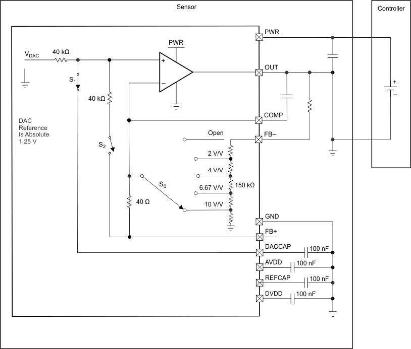
 Figure 42. 0- to 10-V Absolute Output With Internal Drive Diagram
8.1.2.1 Design Requirements
There are only a few requirements to take into account when using the PGA300 in a design:
- Do not exceed the maximum slew rate of 0.5 V/µs at the VDD pin.
- Place a 100-nF capacitor from the AVDD pin to ground, as close as possible to the AVDD pin.
- Place a 100-nF capacitor from the DVDD pin to ground, as close as possible to the DVDD pin.
- Place a capacitor between 10 nF and 1000 nF from the REFCAP pin to ground, as close as possible to the REFCAP pin.
- Implement compensation, using the COMP pin and an isolation resistor, when driving large capacitive loads with the OUT pin.
8.1.2.2 Detailed Design Procedure
8.1.2.2.1 Programmer Tips
8.1.2.2.1.1 Resetting the Microprocessor and Enable Digital Interface
The following bits must be configured to reset the M0 microprocessor and to enable digital interface:
- Set the IF_SEL bit in the MICRO_INTERFACE_CONTROL register to 1.
- Set the MICRO_RESET bit in the MICRO_INTERFACE_CONTROL register to 1.
8.1.2.2.1.2 Turning On the Accurate Reference Buffer (REFCAP Voltage)
The following bits must be configured to turn ON the accurate reference buffer:
- Set the SD bit in the ALPWR register to 0.
- Set the ADC_EN_VREF bit in the ALPWR register to 1.
By turning on the accurate reference buffer, the reference voltage can be measured on REFCAP pin. Further, the capacitor on the REFCAP pin is connected to the reference buffer.
8.1.2.2.1.3 Turning On DAC and DAC GAIN
The following bits must be configured to turn on DAC and DAC GAIN:
- Set the SD bit in the ALPWR register to 0.
- Set the ADC_EN_VREF bit in the ALPWR register to 1.
- Set the DAC_ENABLE bit in the DAC_CTRL_STATUS register to 1.
- Set the 4_20_MA_EN bit in the OP_STAGE_CTRL register for voltage output or current output mode.
- Set the DACCAP_EN bit in the OP_STAGE_CTRL register to connect or disconnect the external capacitor at the DAC output.
- Set the DAC_RATIOMETRIC bit in the DAC_CONFIG register for ratiometric or absolute-voltage output mode.
- Set the TEST_MUX_DAC_EN bit in the AMUX_CTRL register to 1.
8.1.3 0- to 5-V Ratiometric Output With Internal Drive
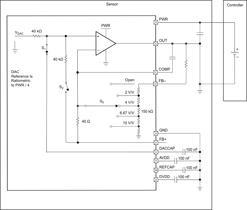
 Figure 43. 0- to 5-V Ratiometric Output With Internal Drive Diagram
8.1.3.1 Design Requirements
There are only a few requirements to take into account when using the PGA300 in a design:
- Do not exceed the maximum slew rate of 0.5 V/µs at the PWR pin.
- Place a 100-nF capacitor from the AVDD pin to ground, as close as possible to the AVDD pin.
- Place a 100-nF capacitor from the DVDD pin to ground, as close as possible to the DVDD pin.
- Place a capacitor between 10 nF and 1000 nF from the REFCAP pin to ground, as close as possible to the REFCAP pin.
- Implement compensation, using the COMP pin and an isolation resistor, when driving large capacitive loads with the OUT pin.
8.1.3.2 Detailed Design Procedure
8.1.3.2.1 Programmer Tips
8.1.3.2.1.1 Resetting the Microprocessor and Enable Digital Interface
The following bits must be configured to reset the M0 microprocessor and to enable digital interface:
- Set the IF_SEL bit in the MICRO_INTERFACE_CONTROL register to 1.
- Set the MICRO_RESET bit in the MICRO_INTERFACE_CONTROL register to 1.
8.1.3.2.1.2 Turning On the Accurate Reference Buffer (REFCAP Voltage)
The following bits must be configured to turn ON the accurate reference buffer:
- Set the SD bit in the ALPWR register to 0.
- Set the ADC_EN_VREF bit in the ALPWR register to 1.
By turning on the accurate reference buffer, the reference voltage can be measured on REFCAP pin. Further, the capacitor on the REFCAP pin is connected to the reference buffer.
8.1.3.2.1.3 Turning On DAC and DAC GAIN
The following bits must be configured to turn on DAC and DAC GAIN:
- Set the SD bit in ALPWR register to 0.
- Set the ADC_EN_VREF bit in the ALPWR register to 1.
- Set the DAC_ENABLE bit in the DAC_CTRL_STATUS register to 1.
- Set the 4_20_MA_EN bit in the OP_STAGE_CTRL register for the voltage-output or current-output mode.
- Set the DACCAP_EN bit in the OP_STAGE_CTRL register to connect or disconnect the external capacitor at the DAC output.
- Set the DAC_RATIOMETRIC bit in the DAC_CONFIG register for ratiometric or absolute-voltage output mode.
- Set the TEST_MUX_DAC_EN bit in the AMUX_CTRL register to 1.