ZHCS019J January 2011 – March 2021 OPA2836 , OPA836
PRODUCTION DATA
- 1 特性
- 2 应用
- 3 说明
- 4 Revision History
- 5 Device Comparison Table
- 6 Pin Configuration and Functions
-
7 Specifications
- 7.1 Absolute Maximum Ratings
- 7.2 ESD Ratings
- 7.3 Recommended Operating Conditions
- 7.4 Thermal Information: OPA836
- 7.5 Thermal Information: OPA2836
- 7.6 Electrical Characteristics: VS = 2.7 V
- 7.7 Electrical Characteristics: VS = 5 V
- 7.8 Typical Characteristics: VS = 2.7 V
- 7.9 Typical Characteristics: VS = 5 V
- 8 Detailed Description
-
9 Application and Implementation
- 9.1
Application Information
- 9.1.1 Noninverting Amplifier
- 9.1.2 Inverting Amplifier
- 9.1.3 Instrumentation Amplifier
- 9.1.4 Attenuators
- 9.1.5 Single-Ended-to-Differential Amplifier
- 9.1.6 Differential-to-Signal-Ended Amplifier
- 9.1.7 Differential-to-Differential Amplifier
- 9.1.8 Gain Setting With OPA836 RUN Integrated Resistors
- 9.1.9 Pulse Application With Single-Supply
- 9.1.10 ADC Driver Performance
- 9.2 Typical Applications
- 9.1
Application Information
- 10Power Supply Recommendations
- 11Layout
- 12Device and Documentation Support
- 13Mechanical, Packaging, and Orderable Information
封装选项
机械数据 (封装 | 引脚)
散热焊盘机械数据 (封装 | 引脚)
- RUN|10
订购信息
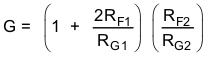
9.1.3 Instrumentation Amplifier
Figure 9-1 is an instrumentation amplifier that combines the high input impedance of the differential-to-differential amplifier circuit and the common-mode rejection of the differential-to-single-ended amplifier circuit. This circuit is often used in applications where high input impedance is required (such as taps from a differential line) or in cases where the signal source has a high output impedance.
If VIN+ = VCM + VSIG+ and VIN– = VCM + VSIG– , then the output of the amplifier may be calculated according to Equation 3.
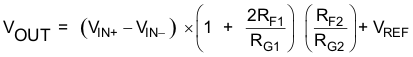
The signal gain of the circuit is set by
 . VCM is rejected, and VREF provides a level shift around which the output signal swings. The single-ended output signal is in-phase with the differential input signal.
 Figure 9-1 Instrumentation Amplifier
Integrated solutions are available, but the OPA836 device provides a much lower-power, high-frequency solution. For best CMRR performance, resistors must be matched. A good guideline to follow is CMRR ≈ the resistor tolerance; so, 0.1% tolerance will provide approximately 60-dB CMRR.