ZHCS019J January 2011 – March 2021 OPA2836 , OPA836
PRODUCTION DATA
- 1 特性
- 2 应用
- 3 说明
- 4 Revision History
- 5 Device Comparison Table
- 6 Pin Configuration and Functions
-
7 Specifications
- 7.1 Absolute Maximum Ratings
- 7.2 ESD Ratings
- 7.3 Recommended Operating Conditions
- 7.4 Thermal Information: OPA836
- 7.5 Thermal Information: OPA2836
- 7.6 Electrical Characteristics: VS = 2.7 V
- 7.7 Electrical Characteristics: VS = 5 V
- 7.8 Typical Characteristics: VS = 2.7 V
- 7.9 Typical Characteristics: VS = 5 V
- 8 Detailed Description
-
9 Application and Implementation
- 9.1
Application Information
- 9.1.1 Noninverting Amplifier
- 9.1.2 Inverting Amplifier
- 9.1.3 Instrumentation Amplifier
- 9.1.4 Attenuators
- 9.1.5 Single-Ended-to-Differential Amplifier
- 9.1.6 Differential-to-Signal-Ended Amplifier
- 9.1.7 Differential-to-Differential Amplifier
- 9.1.8 Gain Setting With OPA836 RUN Integrated Resistors
- 9.1.9 Pulse Application With Single-Supply
- 9.1.10 ADC Driver Performance
- 9.2 Typical Applications
- 9.1
Application Information
- 10Power Supply Recommendations
- 11Layout
- 12Device and Documentation Support
- 13Mechanical, Packaging, and Orderable Information
封装选项
机械数据 (封装 | 引脚)
散热焊盘机械数据 (封装 | 引脚)
- RUN|10
订购信息
7.8 Typical Characteristics: VS = 2.7 V
at VS+ = +2.7 V, VS– = 0 V, VOUT = 1 Vpp, RF = 0 Ω, RL = 2 kΩ, G = 1 V/V, input and output referenced to mid-supply, VIN_CM = mid-supply – 0.5 V. TA = 25°C, unless otherwise noted.
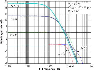 Figure 7-1 Small
Signal Frequency Response
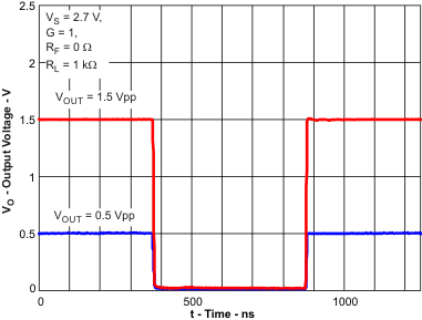 Figure 7-3 Noninverting Pulse Response
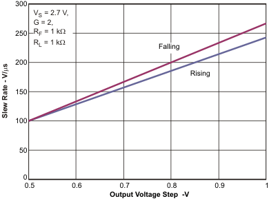 Figure 7-5 Slew
Rate vs Output Voltage Step
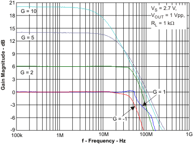 Figure 7-2 Large
Signal Frequency Response
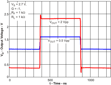 Figure 7-4 Inverting Pulse Response
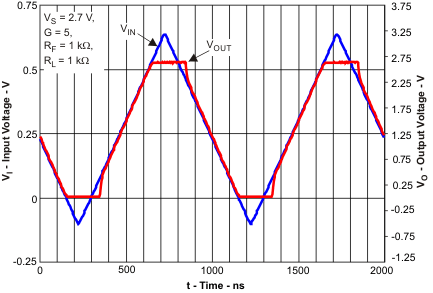 Figure 7-6 Output Overdrive Recovery
at VS+ = +2.7 V, VS– = 0 V, VOUT = 1 Vpp, RF = 0 Ω, RL = 2 kΩ, G = 1 V/V, input and output referenced to mid-supply, VIN_CM = mid-supply – 0.5 V. TA = 25°C, unless otherwise noted.
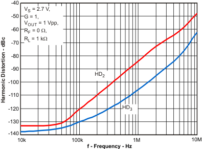 Figure 7-7 Harmonic Distortion vs Frequency
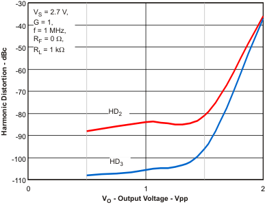 Figure 7-9 Harmonic Distortion vs Output Voltage
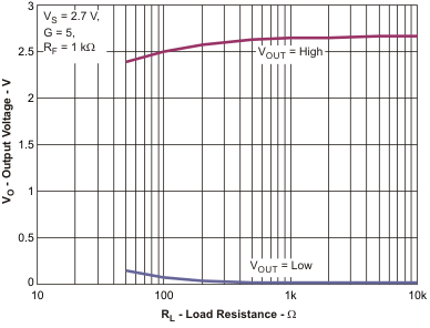 Figure 7-11 Output Voltage Swing vs Load Resistance
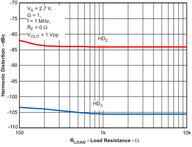 Figure 7-8 Harmonic Distortion vs Load Resistance
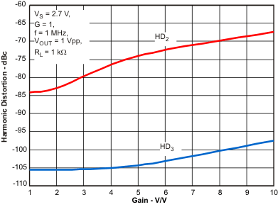 Figure 7-10 Harmonic Distortion vs Gain
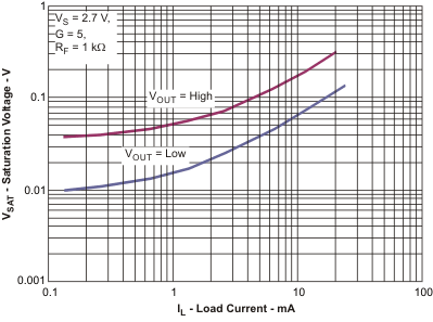 Figure 7-12 Output Saturation Voltage vs Load Current
at VS+ = +2.7 V, VS– = 0 V, VOUT = 1 Vpp, RF = 0 Ω, RL = 2 kΩ, G = 1 V/V, input and output referenced to mid-supply, VIN_CM = mid-supply – 0.5 V. TA = 25°C, unless otherwise noted.
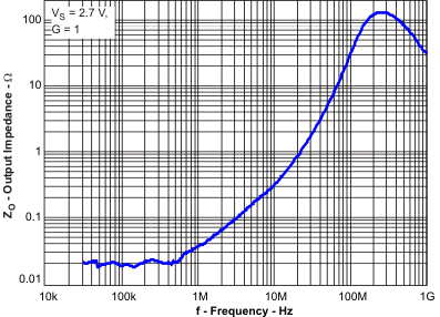 Figure 7-13 Output Impedance vs Frequency
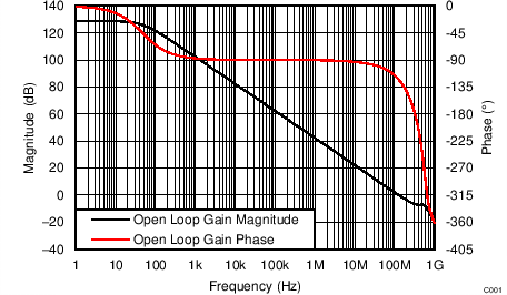
| VS = 2.7 V |
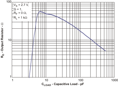 Figure 7-17 Series Output Resistor vs Capacitive Load
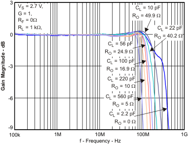 Figure 7-14 Frequency Response With Capacitive Load
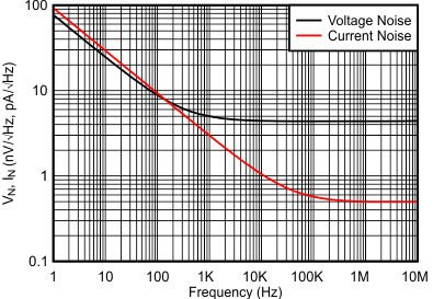
| VS = 2.7 V |
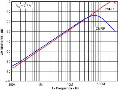 Figure 7-18 Common Mode/Power Supply Rejection Ratios vs Frequency
at VS+ = +2.7 V, VS– = 0 V, VOUT = 1 Vpp, RF = 0 Ω, RL = 2 kΩ, G = 1 V/V, input and output referenced to mid-supply, VIN_CM = mid-supply – 0.5 V. TA = 25°C, unless otherwise noted.
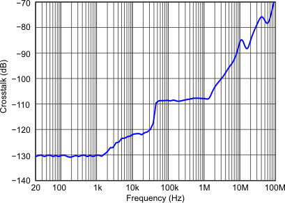 Figure 7-19 Crosstalk vs Frequency
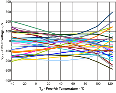 Figure 7-21 Input
Offset Voltage vs Free-Air Temperature
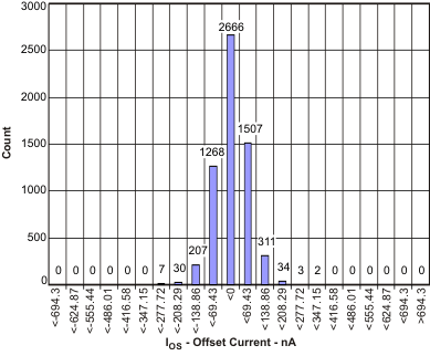 Figure 7-23 Input
Offset Voltage
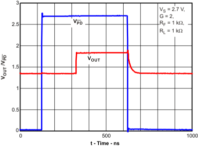 Figure 7-20 Power
Down Response
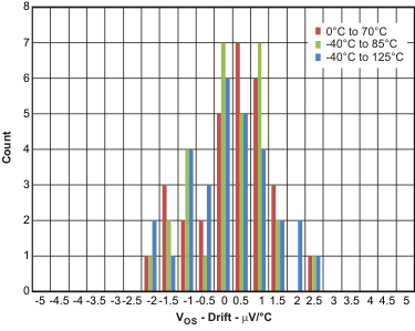 Figure 7-22 Input
Offset Voltage Drift
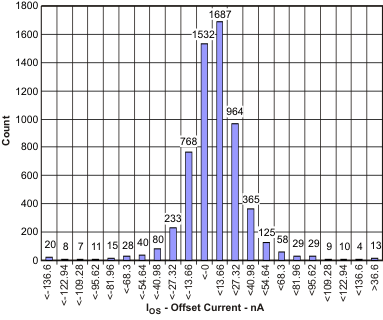 Figure 7-24 Input
Offset Current
Figure 7-24 Input
Offset Currentat VS+ = +2.7 V, VS– = 0 V, VOUT = 1 Vpp, RF = 0 Ω, RL = 2 kΩ, G = 1 V/V, input and output referenced to mid-supply, VIN_CM = mid-supply – 0.5 V. TA = 25°C, unless otherwise noted.
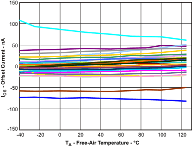 Figure 7-25 Input
Offset Current vs Free-Air Temperature
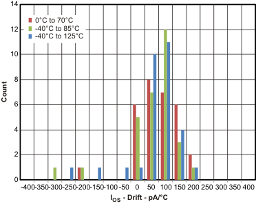 Figure 7-26 Input
Offset Current Drift