SBOS100B July 1999 – January 2016 OPA551 , OPA552
PRODUCTION DATA.
- 1 Features
- 2 Applications
- 3 Description
- 4 Revision History
- 5 Pin Configuration and Functions
- 6 Specifications
- 7 Detailed Description
- 8 Application and Implementation
- 9 Power Supply Recommendations
- 10Layout
- 11Device and Documentation Support
- 12Mechanical, Packaging, and Orderable Information
封装选项
机械数据 (封装 | 引脚)
散热焊盘机械数据 (封装 | 引脚)
订购信息
6 Specifications
6.1 Absolute Maximum Ratings(1)
over operating free-air temperature range (unless otherwise noted)| MIN | MAX | UNIT | |
|---|---|---|---|
| Supply, VS = (V+) to (V–) | 60 | V | |
| Input voltage range, VIN | (V–) – 0.5 | (V+) + 0.5 | V |
| Output | See SOA Curve (Safe Operating Area) | ||
| Operating temperature, TA | –55 | 125 | °C |
| Junction temperature, TJ | 150 | °C | |
| Storage temperature, Tstg | –65 | 150 | °C |
(1) Stresses beyond those listed under Absolute Maximum Ratings may cause permanent damage to the device. These are stress ratings only, which do not imply functional operation of the device at these or any other conditions beyond those indicated under Recommended Operating Conditions. Exposure to absolute-maximum-rated conditions for extended periods may affect device reliability.
6.2 ESD Ratings
| VALUE | UNIT | |||
|---|---|---|---|---|
| V(ESD) | Electrostatic discharge | Human-body model (HBM), per ANSI/ESDA/JEDEC JS-001(1) | ±3000 | V |
(1) JEDEC document JEP155 states that 500-V HBM allows safe manufacturing with a standard ESD control process.
6.3 Recommended Operating Conditions
over operating free-air temperature range (unless otherwise noted)| MIN | MAX | UNIT | ||
|---|---|---|---|---|
| VS | Supply voltage | 8 (±4) | 60 (±30) | V |
| Specified temperature | –40 | 125 | °C | |
6.4 Thermal Information
| THERMAL METRIC(1) | OPA551, OPA552 | UNIT | |||
|---|---|---|---|---|---|
| D (SOIC) |
P (PDIP) |
KTW (DDPAK/TO-263) |
|||
| 8 PINS | 8 PINS | 7 PINS | |||
| RθJA | Junction-to-ambient thermal resistance | 96.7 | 44.1 | 22.7 | °C/W |
| RθJC(top) | Junction-to-case (top) thermal resistance | 38.7 | 31.8 | 34.7 | °C/W |
| RθJB | Junction-to-board thermal resistance | 38.2 | 21.4 | 7.7 | °C/W |
| ψJT | Junction-to-top characterization parameter | 3.7 | 9.1 | 3.3 | °C/W |
| ψJB | Junction-to-board characterization parameter | 37.5 | 21.2 | 7.7 | °C/W |
| RθJC(bot) | Junction-to-case (bottom) thermal resistance | — | — | 0.6 | °C/W |
(1) For more information about traditional and new thermal metrics, see the Semiconductor and IC Package Thermal Metrics application report, SPRA953.
6.5 Electrical Characteristics: VS = ±30 V
At TJ = 25°C(1), RL = 3 kΩ connected to ground, and VOUT = 0 V, unless otherwise noted.| PARAMETER | TEST CONDITIONS | MIN | TYP | MAX | UNIT | ||
|---|---|---|---|---|---|---|---|
| OFFSET VOLTAGE | |||||||
| VOS | Input offset voltage | VCM = 0 V, IO = 0 mA | ±1 | ±3 | mV | ||
| TJ = –40°C to 125°C | ±5 | ||||||
| dVOS /dT | Input offset voltage vs temperature | TJ = –40°C to 125°C | ±7 | µV/°C | |||
| PSRR | Input offset voltage vs power supply | VS = ±4 V to ±30 V, VCM = 0 V | 10 | 30 | µV/V | ||
| INPUT BIAS CURRENT | |||||||
| IB | Input bias current | ±20 | ±100 | pA | |||
| IOS | Input offset current | ±3 | ±100 | pA | |||
| NOISE | |||||||
| en | Input voltage noise density | f = 1 kHz | 14 | nV/√Hz | |||
| in | Current noise density | f = 1 kHz | 3.5 | fA/√Hz | |||
| INPUT VOLTAGE RANGE | |||||||
| VCM | Common-mode voltage range | (V–) + 2.5 | (V+) – 2.5 | V | |||
| CMRR | Common-mode rejection ratio | –27.5 V < VCM < +27.5 V | 92 | 102 | dB | ||
| INPUT IMPEDANCE | |||||||
| Differential | 1013 || 2 | Ω || pF | |||||
| Common-mode | 1013 || 6 | Ω || pF | |||||
| OPEN-LOOP GAIN | |||||||
| AOL | Open-loop voltage gain | RL = 3 kΩ, –28 V < VO < +28 V | 110 | 126 | dB | ||
| RL = 3 kΩ, –28 V < VO < +28 V, TJ = –40°C to 125°C |
100 | ||||||
| RL = 300 Ω, –27 V < VO < +27 V | 120 | ||||||
| OPA551 FREQUENCY RESPONSE | |||||||
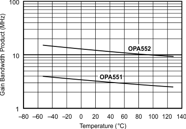
| GBW | Gain-bandwidth product | 3 | MHz | ||||
| SR | Slew rate | G = 1 | ±15 | V/µs | |||
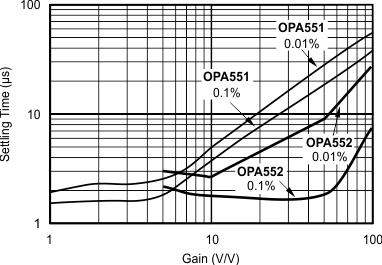
| Settling time | 0.1% | G = 1, CL = 100 pF, 10-V Step | 1.3 | µs | |||
| 0.01% | G = 1, CL = 100 pF, 10-V Step | 2 | |||||
| THD+N | Total harmonic distortion + noise | f = 1 kHz, VO = 15 VRMS, RL = 3 kΩ, G = 3 |
0.0005% | ||||
| f = 1 kHz, VO = 15 VRMS, RL = 300 kΩ, G = 3 |
0.0005% | ||||||
| Overload recovery time | VIN × Gain = VS | 1 | µs | ||||
| OPA552 FREQUENCY RESPONSE | |||||||
| GBW | Gain-bandwidth product | 12 | MHz | ||||
| SR | Slew rate | G = 5 | ±24 | V/µs | |||
| Settling time | 0.1% | G = 5, CL = 100 pF, 10-V Step | 2.2 | µs | |||
| 0.01% | G = 5, CL = 100 pF, 10-V Step | 3 | |||||
| THD+N | Total harmonic distortion + noise | f = 1 kHz, VO = 15 VRMS, RL = 3 kΩ, G = 5 |
0.0005% | ||||
| f = 1 kHz, VO = 15 VRMS, RL = 300 kΩ, G = 5 |
0.0005% | ||||||
| Overload recovery time | VIN × Gain = VS | 1 | µs | ||||
| OUTPUT | |||||||
| VOUT | Voltage output | IO = 200 mA | (V–) + 3 | (V+) – 3 | V | ||
| IO = 200 mA TJ = –40°C to 125°C |
(V–) + 3.5 | (V+) – 3.5 | |||||
| IO = 10 mA | (V–) + 2 | (V+) – 2 | |||||
| IO = 10 mA TJ = –40°C to 125°C |
(V–) + 2.5 | (V+) – 2.7 | |||||
| IO | Maximum continuous current output: DC | Package dependent — see Power Dissipation section | ±200 | mA | |||
| ISC | Short-circuit current | ±380 | mA | ||||
| CLOAD | Capacitive load drive | Stable operation | See Figure 19 | ||||
| SHUTDOWN FLAG | |||||||
| Thermal shutdown status output | Normal operation, sourcing | 0.05 | 1 | µA | |||
| Thermal shutdown, sourcing | 80 | 120 | 160 | ||||
| Voltage compliance range | V– | (V+) –1.5 | V | ||||
| Junction temperature | Shutdown | 160 | °C | ||||
| Reset from shutdown | 140 | ||||||
| POWER SUPPLY | |||||||
| VS | Specified voltage | ±30 | V | ||||
| Operating voltage range | ±4 | ±30 | V | ||||
| IQ | Quiescent current | IO = 0 mA | ±7 | ±8.5 | mA | ||
| TJ = –40°C to 125°C | ±10 | ||||||
| TEMPERATURE RANGE | |||||||
| TJ | Specified range | –40 | 125 | °C | |||
| Operating range | –55 | 125 | |||||
(1) All tests are high-speed tested at 25°C ambient temperature. Effective junction temperature is 25°C unless otherwise noted.
6.6 Typical Characteristics
At TJ = 25°C, VS = ±30 V and RL = 3 kΩ, unless otherwise noted.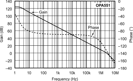
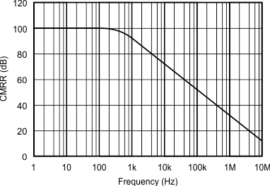
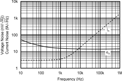
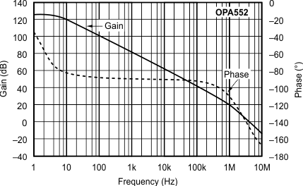
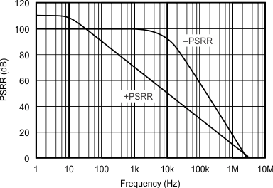
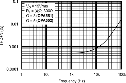
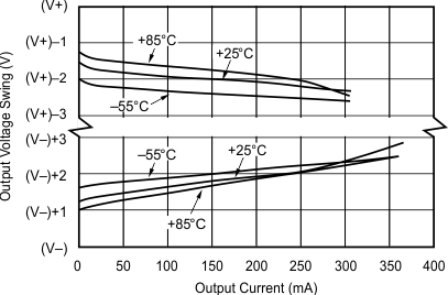
vs Frequency
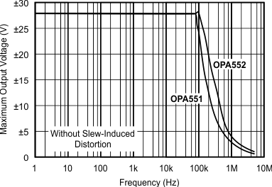
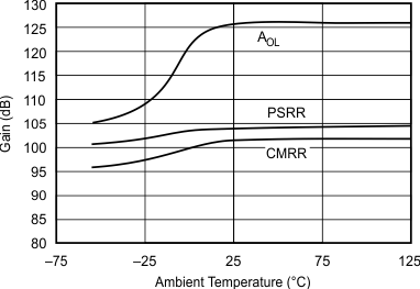
and Common-Mode Rejection Ratio vs Temperature
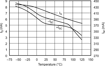
1.
Figure 11. Quiescent Current and Short-Circuit Currentvs Temperature
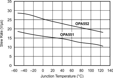
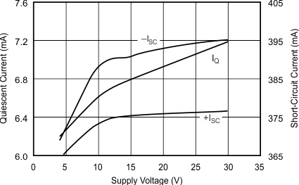
vs Supply Voltage
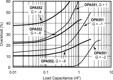
vs Load Capacitance
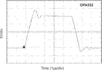
| G = 1, CL = 100 pF |
OPA552
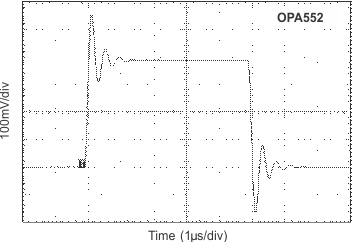
| G = 1, CL = 100 pF |
OPA552
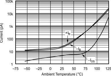
vs Temperature
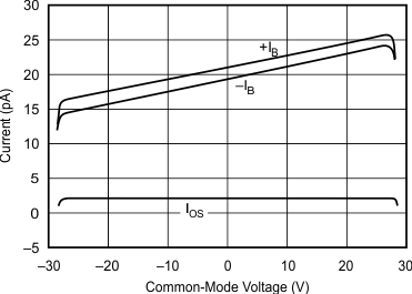
vs Common-Mode Voltage
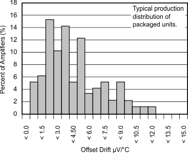
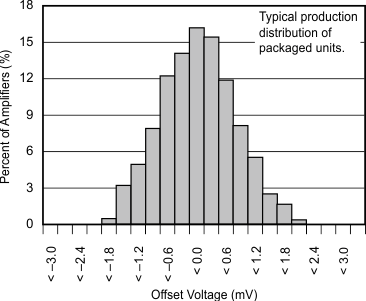 Figure 16. Offset Voltage Production Distribution
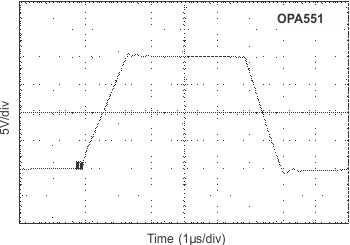
| G = 1, CL = 100 pF | ||
OPA551
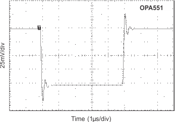
| G = 1, CL = 100 pF |
OPA551
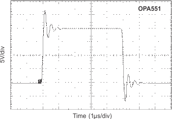
| G = 1, CL = 1000 pF |
OPA551