SBOS100B July   1999  – January 2016 OPA551 , OPA552

PRODUCTION DATA.  

  1. Features
  2. Applications
  3. Description
  4. Revision History
  5. Pin Configuration and Functions
  6. Specifications
    1. 6.1 Absolute Maximum Ratings
    2. 6.2 ESD Ratings
    3. 6.3 Recommended Operating Conditions
    4. 6.4 Thermal Information
    5. 6.5 Electrical Characteristics: VS = ±30 V
    6. 6.6 Typical Characteristics
  7. Detailed Description
    1. 7.1 Overview
    2. 7.2 Functional Block Diagram
    3. 7.3 Feature Description
      1. 7.3.1 Current Limit
      2. 7.3.2 Input Protection
      3. 7.3.3 Thermal Protection
    4. 7.4 Device Functional Modes
  8. Application and Implementation
    1. 8.1 Application Information
    2. 8.2 Typical Application
      1. 8.2.1 Design Requirements
      2. 8.2.2 Detailed Design Procedure
        1. 8.2.2.1 Capacitive Loads
        2. 8.2.2.2 Increasing Output Current
        3. 8.2.2.3 Using the OPA552 in Low Gains
        4. 8.2.2.4 Offset Voltage Error Calculation
      3. 8.2.3 Application Curve
  9. Power Supply Recommendations
    1. 9.1 Power Supplies
  10. 10Layout
    1. 10.1 Layout Guidelines
    2. 10.2 Layout Example
    3. 10.3 Power Dissipation
    4. 10.4 Safe Operating Area
    5. 10.5 Heat Sinking
  11. 11Device and Documentation Support
    1. 11.1 Device Support
      1. 11.1.1 Third-Party Products Disclaimer
    2. 11.2 Documentation Support
      1. 11.2.1 Related Links
      2. 11.2.2 Related Documentation
    3. 11.3 Community Resources
    4. 11.4 Trademarks
    5. 11.5 Electrostatic Discharge Caution
    6. 11.6 Glossary
  12. 12Mechanical, Packaging, and Orderable Information

封装选项

机械数据 (封装 | 引脚)
散热焊盘机械数据 (封装 | 引脚)
订购信息

5 Pin Configuration and Functions

OPA551, OPA552 P Package
8-Pin PDIP
Top View
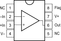
OPA551 OPA552 pinout_01_sbos100.gif
OPA551, OPA552 D Package
8-Pin SOIC
Top View
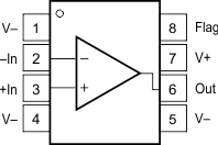
OPA551 OPA552 pinout_02_sbos100.gif
OPA551, OPA552 KTW Package
7-Pin DDPAK/TO-263 Surface-Mount
Top View
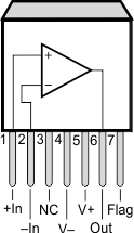
OPA551 OPA552 DDPAK_7_surface_mount_sbos100.gif

NOTE:

Tab is connected to V– supply.

Pin Functions

PIN I/O DESCRIPTION
NAME SOIC PDIP DDPAK/
TO-263
Flag 8 8 7 O Thermal shutdown indicator
+IN 3 3 1 I Noninverting input
–IN 2 2 2 I Inverting input
NC 1, 5 3 No internal connection (can be left floating)
Out 6 6 6 O Output
Tab Tab Connect to V– supply
V+ 7 7 5 Positive (highest) power supply
V– 1, 4, 5 4 4 Negative (lowest) power supply