ZHCSI16F March   2002  – April 2018 OPA2357 , OPA357

PRODUCTION DATA.  

  1. 特性
  2. 应用
  3. 说明
    1.     Device Images
      1.      简化原理图
  4. 修订历史记录
  5. Pin Configuration and Functions
    1.     Pin Functions
  6. Specifications
    1. 6.1 Absolute Maximum Ratings
    2. 6.2 ESD Ratings
    3. 6.3 Recommended Operating Conditions
    4. 6.4 Thermal Information
    5. 6.5 Electrical Characteristics: VS = +2.7-V to +5.5-V Single-Supply
    6. 6.6 Typical Characteristics
  7. Detailed Description
    1. 7.1 Overview
    2. 7.2 Functional Block Diagram
    3. 7.3 Feature Description
      1. 7.3.1  OPAx357 Comparison
      2. 7.3.2  Operating Voltage
      3. 7.3.3  Enable Function
      4. 7.3.4  Rail-to-Rail Input
      5. 7.3.5  Rail-to-Rail Output
      6. 7.3.6  Output Drive
      7. 7.3.7  Video
      8. 7.3.8  Wideband Video Multiplexing
      9. 7.3.9  Driving Analog-to-Digital Converters
      10. 7.3.10 Capacitive Load and Stability
      11. 7.3.11 Wideband Transimpedance Amplifier
    4. 7.4 Device Functional Modes
  8. Application and Implementation
    1. 8.1 Application Information
    2. 8.2 Typical Applications
      1. 8.2.1 Transimpedance Amplifier
        1. 8.2.1.1 Design Requirements
        2. 8.2.1.2 Detailed Design Procedure
          1. 8.2.1.2.1 Custom Design With WEBENCH® Tools
          2. 8.2.1.2.2 OPAx357 Design Procedure
            1. 8.2.1.2.2.1 Optimizing the Transimpedance Circuit
        3. 8.2.1.3 Application Curve
      2. 8.2.2 High-Impedance Sensor Interface
      3. 8.2.3 Driving ADCs
      4. 8.2.4 Active Filter
  9. Power Supply Recommendations
    1. 9.1 Power Dissipation
  10. 10Layout
    1. 10.1 Layout Guidelines
    2. 10.2 Layout Example
  11. 11器件和文档支持
    1. 11.1 器件支持
      1. 11.1.1 开发支持
        1. 11.1.1.1 使用 WEBENCH® 工具创建定制设计
    2. 11.2 文档支持
      1. 11.2.1 相关文档
    3. 11.3 相关链接
    4. 11.4 接收文档更新通知
    5. 11.5 社区资源
    6. 11.6 商标
    7. 11.7 静电放电警告
    8. 11.8 Glossary
  12. 12机械、封装和可订购信息

封装选项

机械数据 (封装 | 引脚)
散热焊盘机械数据 (封装 | 引脚)
订购信息

Driving Analog-to-Digital Converters

The OPA357 series op amps offer 60 ns of settling time to 0.01%, making the series a good choice for driving high- and medium-speed sampling A/D converters and reference circuits. The OPA357 series provides an effective means of buffering the A/D converter input capacitance and resulting charge injection while providing signal gain.

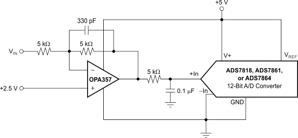
Figure 38 shows the OPA357 driving an A/D converter. With the OPA357 in an inverting configuration, a capacitor across the feedback resistor can be used to filter high-frequency noise in the signal, as shown in Figure 38.
OPA357 OPA2357 OPA357_SBOS235_inverting_configuration_driving_adc.gif

NOTE:

A/D converter input = 0 V to VREF.

NOTE:

VIN = 0 V to –5 V for a 0-V to 5-V output.
Figure 38. The OPA357 in Inverting Configuration Driving an A/D Converter