ZHCSF20A May 2016 – May 2016 OPA2377-Q1 , OPA377-Q1 , OPA4377-Q1
PRODUCTION DATA.
8 Application and Implementation
NOTE
Information in the following applications sections is not part of the TI component specification, and TI does not warrant its accuracy or completeness. TI’s customers are responsible for determining suitability of components for their purposes. Customers should validate and test their design implementation to confirm system functionality.
8.1 Application Information
The OPAx377-Q1 family of operational amplifiers is built on a precision analog CMOS technology featuring low noise and low offset voltage. The OPAx377-Q1 family delivers excellent offset voltage (250 μV, typical). Additionally, the amplifier boasts a fast slew rate, low drift, low noise, and excellent PSRR and AOL. These 5.5-MHz CMOS op amps operate on 760 μA (typical) quiescent current.
8.2 Typical Application
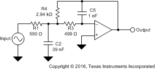
Low-pass filters are commonly employed in signal processing applications to reduce noise and prevent aliasing. The OPA377-Q1 is ideally suited to construct high-speed, high-precision active filters. Figure 25 shows a second-order, low-pass filter commonly encountered in signal processing applications.
 Figure 25. Typical Application Schematic
8.2.1 Design Requirements
Use the following parameters for this design example:
- Gain = 5 V/V (inverting gain)
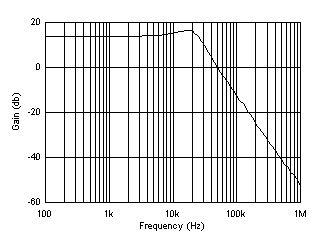
- Low-pass cutoff frequency = 25 kHz
- Second-order Chebyshev filter response with 3-dB gain peaking in the passband
8.2.2 Detailed Design Procedure
The infinite-gain multiple-feedback circuit for a low-pass network function is shown in Figure 25. Use Equation 1 to calculate the voltage transfer function.

This circuit produces a signal inversion. For this circuit, the gain at dc and the low-pass cutoff frequency are calculated by Equation 2:

Software tools are readily available to simplify filter design. WEBENCH® Filter Designer is a simple, powerful, and easy-to-use active filter design program. The WEBENCH Filter Designer lets you create optimized filter designs using a selection of TI operational amplifiers and passive components from TI's vendor partners.
Available as a web-based tool from the WEBENCH® Design Center, WEBENCH® Filter Designer allows to design, optimize, and simulate complete multi-stage active filter solutions within minutes.
8.2.3 Application Curve
 Figure 26. Low-Pass Filter Transfer Function