ZHCSF20A May 2016 – May 2016 OPA2377-Q1 , OPA377-Q1 , OPA4377-Q1
PRODUCTION DATA.
5 Pin Configuration and Functions
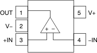
OPA377-Q1: DBV Package
5-Pin SOT23
Top View

Pin Functions: OPA377-Q1
| PIN | I/O | DESCRIPTION | |
|---|---|---|---|
| NAME | NO. | ||
| DBV | |||
| +IN | 3 | I | Noninverting input |
| –IN | 4 | I | Inverting input |
| NC | — | — | No internal connection (can be left floating) |
| OUT | 1 | O | Output |
| V– | 2 | — | Negative (lowest) power supply |
| V+ | 5 | — | Positive (highest) power supply |
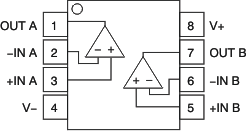
OPA2377-Q1: DGK Package
8-Pin VSSOP and SOIC
Top View

Pin Functions: OPA2377-Q1
| PIN | I/O | DESCRIPTION | |
|---|---|---|---|
| NAME | NO. | ||
| DGK | |||
| –IN A | 2 | I | Inverting input, channel A |
| –IN B | 6 | I | Inverting input, channel B |
| +IN A | 3 | I | Noninverting input, channel A |
| +IN B | 5 | I | Noninverting input, channel B |
| OUT A | 1 | O | Output, channel A |
| OUT B | 7 | O | Output, channel B |
| V– | 4 | — | Negative (lowest) power supply |
| V+ | 8 | — | Positive (highest) power supply |
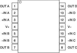
OPA4377-Q1: PW Package
14-Pin TSSOP
Top View

Pin Functions: OPA4377-Q1
| PIN | I/O | DESCRIPTION | |
|---|---|---|---|
| NAME | NO. | ||
| PW | |||
| –IN A | 2 | I | Inverting input, channel A |
| –IN B | 6 | I | Inverting input, channel B |
| –IN C | 9 | I | Inverting input, channel C |
| –IN D | 13 | I | Inverting input, channel D |
| +IN A | 3 | I | Noninverting input, channel A |
| +IN B | 5 | I | Noninverting input, channel B |
| +IN C | 10 | I | Noninverting input, channel C |
| +IN D | 12 | I | Noninverting input, channel D |
| OUT A | 1 | O | Output, channel A |
| OUT B | 7 | O | Output, channel B |
| OUT C | 8 | O | Output, channel C |
| OUT D | 14 | O | Output, channel D |
| V– | 11 | — | Negative (lowest) power supply |
| V+ | 4 | — | Positive (highest) power supply |