ZHCSD45 December 2014 OPA2277-EP
PRODUCTION DATA.
9 Application and Implementation
NOTE
Information in the following applications sections is not part of the TI component specification, and TI does not warrant its accuracy or completeness. TI’s customers are responsible for determining suitability of components for their purposes. Customers should validate and test their design implementation to confirm system functionality.
9.1 Application Information
The OPA2277 is unity-gain stable and free from unexpected output phase reversal, making it easy to use in a wide range of applications. Applications with noisy or high-impedance power supplies may require decoupling capacitors close to the device pins. In most cases, 0.1-μF capacitors are adequate.
9.2 Typical Application
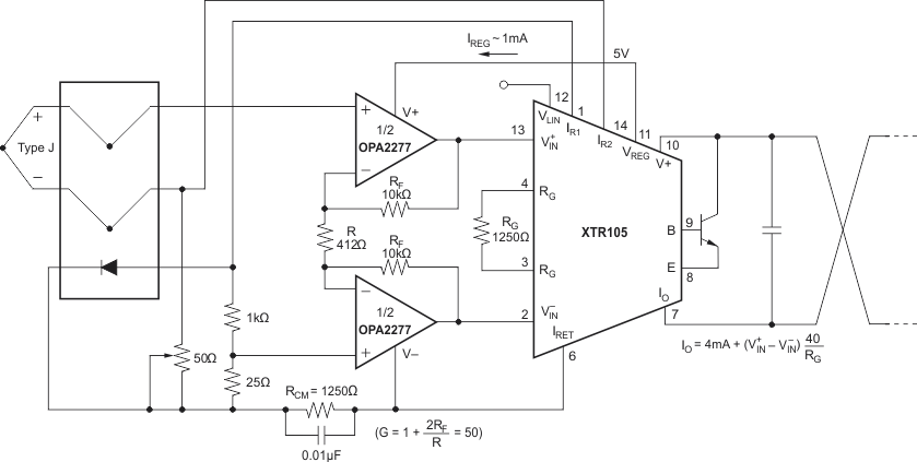 Figure 21. Thermocouple Low-Offset, Low-Drift Loop Measurement With Diode Cold Junction Compensation
9.2.1 Design Requirements
For the thermocouple low-offset, low-drift loop measurement with diode cold junction compensation (see Figure 21), Table 1 lists the design parameters needed with gain = 50.
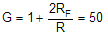
Table 1. Design Parameters
| DESIGN PARAMETER | EXAMPLE VALUE |
|---|---|
| RF | 10 kΩ |
| R | 412 Ω |
9.2.2 Detailed Design Procedure
9.2.2.1 Offset Voltage Adjustment
The OPA2277 is laser-trimmed for very-low offset voltage and drift so most circuits do not require external adjustment. However, offset voltage trim connections are provided on pins 1 and 8. Offset voltage can be adjusted by connecting a potentiometer as shown in Figure 22. Only use this adjustment to null the offset of the operational amplifier. Do not use this adjustment to compensate for offsets created elsewhere in a system because this can introduce additional temperature drift.
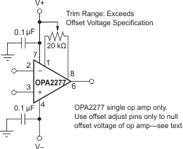 Figure 22. OPA2277 Offset Voltage Trim Circuit
9.2.2.2 Input Protection
The inputs of the OPA2277 are protected with 1-kΩ series input resistors and diode clamps. The inputs can withstand ±30-V differential inputs without damage. The protection diodes conduct current when the inputs are overdriven. This may disturb the slewing behavior of unity-gain follower applications, but does not damage the operational amplifier.
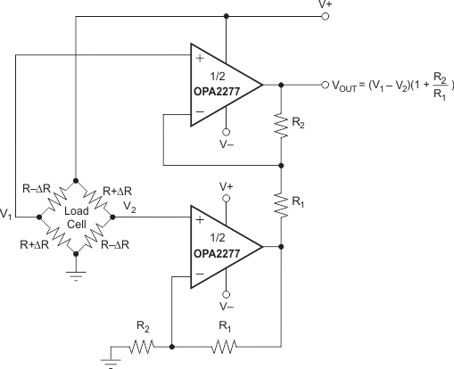
9.2.2.3 Input Bias Current Cancellation
The input stage base current of the OPA2277 is internally compensated with an equal and opposite cancellation circuit. The resulting input bias current is the difference between the input stage base current and the cancellation current. This residual input bias current can be positive or negative.
When the bias current is canceled in this manner, the input bias current and input offset current are approximately the same magnitude. As a result, it is not necessary to use a bias current cancellation resistor as is often done with other operational amplifiers (see Figure 23). A resistor added to cancel input bias current errors may actually increase offset voltage and noise.
 Figure 23. Input Bias Current Cancellation
9.2.3 Application Curves
At TJ = 25°C, VS = ±15 V, and RL = 2 kΩ. Figure 25 shows Change in input bias current versus power supply voltage. Curve shows normalized change in bias current with respect to VS = ±10 V (+20 V). Typical IB may range from –0.5 to 0.5 nA at VS = ±10 V. Figure 26 shows change in input bias current versus common-mode voltage. Curve shows normalized change in bias current with respect to VCM = 0 V. Typical IB may range from –0.5 to 0.5 nA at VCM = 0 V.
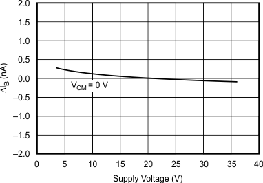 Figure 25. Change in Input Bias Current vs Power Supply Voltage
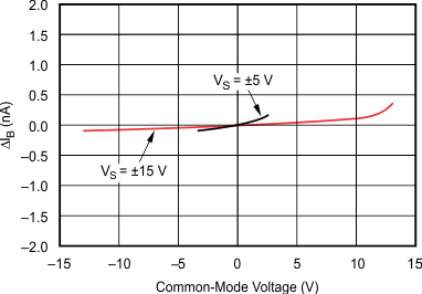 Figure 26. Change in Input Bias Current vs Common-Mode Voltage