ZHCSD45 December 2014 OPA2277-EP
PRODUCTION DATA.
11 Layout
11.1 Layout Guidelines
Solder the lead-frame die pad to a thermal pad on the PCB. Mechanical drawings in 机械封装和可订购信息 show the physical dimensions for the package and pad.
Soldering the exposed pad significantly improves board-level reliability during temperature cycling, key push, package shear, and similar board-level tests. Even with applications that have low-power dissipation, the exposed pad must be soldered to the PCB to provide structural integrity and long-term reliability.
The OPA2277 has very-low offset voltage and drift. To achieve highest performance, optimize circuit layout and mechanical conditions. Offset voltage and drift can be degraded by small thermoelectric potentials at the operational amplifier inputs. Connections of dissimilar metals generate thermal potential which can degrade the ultimate performance of the OPA2277. These thermal potentials can be made to cancel by assuring that they are equal in both input terminals.
- Keep thermal mass of the connections made to the two input terminals similar.
- Locate heat sources as far as possible from the critical input circuitry.
- Shield operational amplifier and input circuitry from air currents such as cooling fans.
11.2 Layout Example
11.2.1 Board Layout
This demonstration fixture is a two-layer PCB. It uses a ground plane on the bottom, and signal and power traces on the top. The ground plane has been opened up around Op Amp pins sensitive to capacitive loading. Power-supply traces are laid out to keep current loop areas to a minimum. The SMA (or SMB) connectors may be mounted either vertically or horizontally.
The location and type of capacitors used for power-supply bypassing are crucial to high-frequency amplifiers. The tantalum capacitors, C1 and C2, do not need to be as close to pins 7 and 4 on your PCB, and may be shared with other amplifiers.
11.2.2 Measurement Tips
This demonstration fixture and the component values shown are designed to operate in a 50Ω environment. Most data sheet plots are obtained in this manner. Change the component values for different input and output impedance levels.
Do not use high-impedance probes; they represent a heavy capacitive load to the Op Amps, and will alter the amplifier response. Instead, use low impedance (≤ 500Ω) probes with adequate bandwidth. The probe input capacitance and resistance set an upper limit on the measurement bandwidth. If a high-impedance probe must be used, place a 100Ω resistor on the probe tip to isolate its capacitance from the circuit.
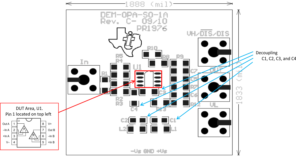 Figure 27. Decoupling Capacitors and DUT Area