ZHCSD40P April 2012 – January 2024 LP5907
PRODUCTION DATA
- 1
- 1 特性
- 2 应用
- 3 说明
- 4 Pin Configuration and Functions
- 5 Specifications
- 6 Detailed Description
- 7 Application and Implementation
- 8 Device and Documentation Support
- 9 Revision History
- 10Mechanical, Packaging, and Orderable Information
封装选项
机械数据 (封装 | 引脚)
散热焊盘机械数据 (封装 | 引脚)
- DQN|4
订购信息
4 Pin Configuration and Functions
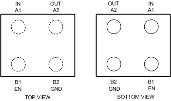
 Figure 4-1 YKE, YKG, YKM, and YCR Packages,4-Pin DSBGA
Table 4-1 Pin Functions: DSBGA
| PIN | TYPE | DESCRIPTION | |
|---|---|---|---|
| DSBGA | NAME | ||
| A1 | IN | I | Input voltage supply. Connect a 1µF capacitor at this input. |
| A2 | OUT | O | Regulated output voltage. Connect a minimum 1µF low-ESR capacitor to this pin. Connect this output to the load circuit. An internal 230Ω (typical) pulldown resistor prevents a charge remaining on VOUT when the regulator is in the shutdown mode (VEN low). |
| B1 | EN | I | Enable input. A low voltage (< VIL) on this pin turns the regulator off and discharges the output pin to GND through an internal 230Ω pulldown resistor. A high voltage (> VIH) on this pin enables the regulator output. This pin has an internal 1MΩ pulldown resistor to hold the regulator off by default. |
| B2 | GND | — | Common ground |
 Figure 4-2 DQN Package,4-Pin X2SON
(Bottom View)
 Figure 4-3 DBV Package,5-Pin SOT-23
(Top View)
Table 4-2 Pin Functions: X2SON, SOT-23
| PIN | TYPE | DESCRIPTION | ||
|---|---|---|---|---|
| NAME | X2SON | SOT-23 | ||
| EN | 3 | 3 | I | Enable input. A low voltage (< VIL) on this pin turns the regulator off and discharges the output pin to GND through an internal 230Ω pulldown resistor. A high voltage (> VIH) on this pin enables the regulator output. This pin has an internal 1MΩ pulldown resistor to hold the regulator off by default. |
| GND | 2 | 2 | — | Common ground. |
| IN | 4 | 1 | I | Input voltage supply. Connect a 1µF capacitor at this input. |
| N/C | — | 4 | — | No internal electrical connection. |
| OUT | 1 | 5 | O | Regulated output voltage. Connect a minimum 1µF low-ESR capacitor to this pin. Connect this output to the load circuit. An internal 230Ω (typical) pulldown resistor prevents a charge remaining on VOUT when the regulator is in shutdown mode (VEN low). |
| Thermal Pad | 5 | — | — | Thermal pad for the X2SON package, connect to GND or leave floating. Do not connect to any potential other than GND. |