SNVS441I January 2007 – November 2016 LP5521
PRODUCTION DATA.
- 1 Features
- 2 Applications
- 3 Description
- 4 Revision History
- 5 Pin Configuration and Functions
-
6 Specifications
- 6.1 Absolute Maximum Ratings
- 6.2 ESD Ratings
- 6.3 Recommended Operating Conditions
- 6.4 Thermal Information
- 6.5 Electrical Characteristics
- 6.6 Charge Pump Electrical Characteristics
- 6.7 LED Driver Electrical Characteristics (R, G, B Outputs)
- 6.8 Logic Interface Characteristics
- 6.9 I2C Timing Requirements (SDA, SCL)
- 6.10 Typical Characteristics
-
7 Detailed Description
- 7.1 Overview
- 7.2 Functional Block Diagram
- 7.3 Feature Description
- 7.4 Device Functional Modes
- 7.5 Programming
- 7.6
Register Maps
- 7.6.1 Enable Register (Enable)
- 7.6.2 Operation Mode Register (OP Mode)
- 7.6.3 R Channel PWM Control (R_PWM)
- 7.6.4 G Channel PWM Control (G_PWM)
- 7.6.5 B Channel PWM Control (B_PWM)
- 7.6.6 R Channel Current (R_CURRENT)
- 7.6.7 G Channel Current (G_CURRENT)
- 7.6.8 B Channel Current (B_CURRENT)
- 7.6.9 Configuration Control (CONFIG)
- 7.6.10 R Channel Program Counter Value (R Channel PC)
- 7.6.11 G Channel Program Counter Value (G Channel PC)
- 7.6.12 B Channel Program Counter Value (B Channel PC)
- 7.6.13 Status/Interrupt Register
- 7.6.14 RESET Register
- 7.6.15 GPO Register
- 7.6.16 Program Memory
- 8 Application and Implementation
- 9 Power Supply Recommendations
- 10Layout
- 11Device and Documentation Support
- 12Mechanical, Packaging, and Orderable Information
5 Pin Configuration and Functions
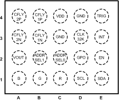
YFQ Package
20-Pin DSBGA
Top View

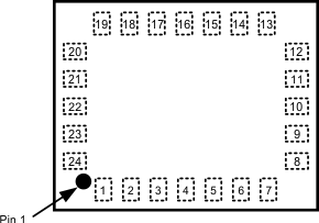
NJA Package
24-Pin WQFN
Top View

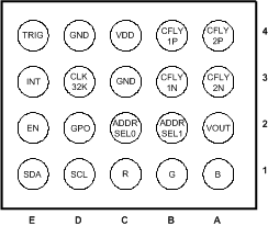
YFQ Package
20-Pin DSBGA
Bottom View

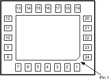
NJA Package
24-Pin WQFN
Bottom View

Pin Functions LP5521TM
| PIN | TYPE(1) | DESCRIPTION | |
|---|---|---|---|
| NUMBER | NAME | ||
| 1A | B | A | Current source output |
| 1B | G | A | Current source output |
| 1C | R | A | Current source output |
| 1D | SCL | I | I2C Serial interface clock input |
| 1E | SDA | I/OD | I2C Serial interface data input/output |
| 2A | VOUT | A | Charge pump output |
| 2B | ADDR_SEL1 | I | I2C address select input |
| 2C | ADDR_SEL0 | I | I2C address select input |
| 2D | GPO | O | General purpose output |
| 2E | EN | I | Chip enable |
| 3A | CFLY2N | A | Negative terminal of charge pump fly capacitor 2 |
| 3B | CFLY1N | A | Negative terminal of charge pump fly capacitor 1 |
| 3C | GND | G | Ground |
| 3D | CLK_32K | I | 32-kHz clock input |
| 3E | INT | OD/O | Interrupt output / General Purpose Output |
| 4A | CFLY2P | A | Positive terminal of charge pump fly capacitor 2 |
| 4B | CFLY1P | A | Positive terminal of charge pump fly capacitor 1 |
| 4C | VDD | P | Power supply pin |
| 4D | GND | G | Ground |
| 4E | TRIG | I/OD | Trigger input/output |
Pin Functions LP5521YQ
| PIN | TYPE(1) | DESCRIPTION | |
|---|---|---|---|
| NUMBER | NAME | ||
| 1 | CFLY2P | A | Positive pin of charge pump fly capacitor 2 |
| 2 | CFLY1P | A | Positive pin of charge pump fly capacitor 1 |
| 3 | VDD | P | Power supply pin |
| 4 | GND | G | Ground |
| 5 | CLK_32K | I | 32-kHz clock input |
| 6 | INT | OD/O | Interrupt output / General purpose output |
| 7 | TRIG | I/OD | Trigger input/output |
| 8 | N/C | ||
| 9 | N/C | ||
| 10 | N/C | ||
| 11 | N/C | ||
| 12 | N/C | ||
| 13 | SDA | I/OD | I2C serial interface data input/output |
| 14 | EN | I | Chip enable |
| 15 | SCL | I | I2C Serial interface clock input |
| 16 | GPO | O | General purpose output |
| 17 | R | A | Current source output |
| 18 | G | A | Current source output |
| 19 | B | A | Current source output |
| 20 | ADDR_SEL0 | I | I2C address select input |
| 21 | ADDR_SEL1 | I | I2C address select input |
| 22 | VOUT | A | Charge pump output |
| 23 | CFLY2N | A | Negative pin of charge pump fly capacitor 2 |
| 24 | CFLY1N | A | Negative pin of charge pump fly capacitor 1 |
(1) A: Analog Pin, G: Ground Pin, P: Power Pin, I: Input Pin, I/O: Input/Output Pin, O: Output Pin, OD: Open Drain Pin