ZHCSJT3B May 2019 – August 2020 LP5009 , LP5012
PRODUCTION DATA
- 1 特性
- 2 应用
- 3 说明
- 4 Revision History
- 5 Description (continued)
- 6 Pin Configuration and Functions
- 7 Specifications
-
8 Detailed Description
- 8.1 Overview
- 8.2 Functional Block Diagram
- 8.3
Feature Description
- 8.3.1 PWM Control for Each Channel
- 8.3.2 LED Bank Control
- 8.3.3 Current Range Setting
- 8.3.4 Automatic Power-Save Mode
- 8.3.5 Protection Features
- 8.4 Device Functional Modes
- 8.5 Programming
- 8.6
Register Maps
- 45
- 8.6.1 DEVICE_CONFIG0 (Address = 0h) [reset = 0h]
- 8.6.2 DEVICE_CONFIG1 (Address = 1h) [reset = 3Ch]
- 8.6.3 LED_CONFIG0 (Address = 2h) [reset = 00h]
- 8.6.4 BANK_BRIGHTNESS (Address = 3h) [reset = FFh]
- 8.6.5 BANK_A_COLOR (Address = 4h) [reset = 00h]
- 8.6.6 BANK_B_COLOR (Address = 5h) [reset = 00h]
- 8.6.7 BANK_C_COLOR (Address = 6h) [reset = 00h]
- 8.6.8 LED0_BRIGHTNESS (Address = 7h) [reset = FFh]
- 8.6.9 LED1_BRIGHTNESS (Address = 8h) [reset = FFh]
- 8.6.10 LED2_BRIGHTNESS (Address = 9h) [reset = FFh]
- 8.6.11 LED3_BRIGHTNESS (Address = 0Ah) [reset = FFh]
- 8.6.12 OUT0_COLOR (Address = 0Bh) [reset = 00h]
- 8.6.13 OUT1_COLOR (Address = 0Ch) [reset = 00h]
- 8.6.14 OUT2_COLOR (Address = 0Dh) [reset = 00h]
- 8.6.15 OUT3_COLOR (Address = 0Eh) [reset = 00h]
- 8.6.16 OUT4_COLOR (Address = 0Fh) [reset = 00h]
- 8.6.17 OUT5_COLOR (Address = 10h) [reset = 00h]
- 8.6.18 OUT6_COLOR (Address = 11h) [reset = 00h]
- 8.6.19 OUT7_COLOR (Address = 12h) [reset = 00h]
- 8.6.20 OUT8_COLOR (Address = 13h) [reset = 00h]
- 8.6.21 OUT9_COLOR (Address = 14h) [reset = 00h]
- 8.6.22 OUT10_COLOR (Address = 15h) [reset = 00h]
- 8.6.23 OUT11_COLOR (Address = 16h) [reset = 00h]
- 8.6.24 RESET (Address = 17h) [reset = 00h]
- 9 Application and Implementation
- 10Power Supply Recommendations
- 11Layout
- 12Device and Documentation Support
- 13Mechanical, Packaging, and Orderable Information
封装选项
机械数据 (封装 | 引脚)
散热焊盘机械数据 (封装 | 引脚)
- RUK|20
订购信息
8.3.2 LED Bank Control
For most LED-animation effects, like blinking and breathing, all the RGB LEDs have the same lighting pattern. Instead of controlling the individual LED separately, which occupies the microcontroller resources heavily, the LP50xx device provides an easy coding approach, the LED bank control.
Each channel can be configured as either independent control or bank control through the LEDx_Bank_EN register. When LEDx_Bank_EN = 0 (default), the LED is controlled independently by the related color-mixing and intensity-control registers. When LEDx_Bank_EN = 1, the LP50xx device drives the LEDs in LED bank-control mode. The LED bank has its own independent PWM control scheme, which is the same structure as the PWM scheme of each channel. See PWM Control for Each Channel for more details. When a channel is configured in LED bank-control mode, the related color mixing and intensity control is governed by the bank control registers (BANK_A_COLOR, BANK_B_COLOR, BANK_C_COLOR, and BANK_BRIGHTNESS) regardless of the inputs on its own color-mixing and intensity-control registers.
 Figure 8-5 Bank PWM Control Scheme
| OUT NUMBER | BANK NUMBER | RGB LED MODULE NUMBER |
|---|---|---|
| OUT0 | Bank A | LED0 |
| OUT1 | Bank B | |
| OUT2 | Bank C | |
| OUT3 | Bank A | LED1 |
| OUT4 | Bank B | |
| OUT5 | Bank C | |
| OUT6 | Bank A | LED2 |
| OUT7 | Bank B | |
| OUT8 | Bank C | |
| OUT9 (LP5012 only) | Bank A | LED3 |
| OUT10 (LP5012 only) | Bank B | |
| OUT11 (LP5012 only) | Bank C |
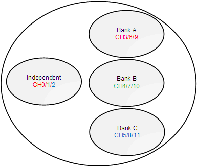
With the bank control configuration, the LP50xx device enables users to achieve smooth and live LED effects globally with an ultrasimple software effort. Figure 8-6 shows an example using LED0 as an independent RGB indicator and others with group breathing effect.
 Figure 8-6 Bank PWM Control Example