SNVS335F December 2006 – November 2016 LP38853
PRODUCTION DATA.
- 1 Features
- 2 Applications
- 3 Description
- 4 Revision History
- 5 Pin Configuration and Functions
- 6 Specifications
- 7 Detailed Description
- 8 Application and Implementation
- 9 Power Supply Recommendations
- 10Layout
- 11Device and Documentation Support
- 12Mechanical, Packaging, and Orderable Information
封装选项
机械数据 (封装 | 引脚)
散热焊盘机械数据 (封装 | 引脚)
订购信息
10 Layout
10.1 Layout Guidelines
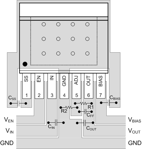
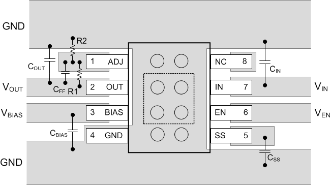
For best overall performance, place all circuit components on the same side of the circuit board and as near as practical to the respective LDO pin connections. Place ground return connections to the input and output capacitor, and to the LDO ground pin as close as possible to each other, connected by a wide, component side, copper surface. The use of vias and long traces to create LDO circuit connections is strongly discouraged and negatively affects system performance. This grounding and layout scheme minimizes inductive parasitic, and thereby reduces load current transients, minimizes noise, and increases circuit stability.
A ground reference plane is also recommended and is either embedded in the PCB itself or located on the bottom side of the PCB opposite the components. This reference plane serves to assure accuracy of the output voltage, shield noise, and behaves similarly to a thermal plane to spread heat from the LDO device when connected to the PowerPAD. In most applications, this ground plane is necessary to meet thermal requirements.
10.2 Layout Examples
 Figure 31. LP38853 DDPAK/TO-263 and TO-220 Layout Example
 Figure 32. LP38853 SO PowerPAD Layout Example