ZHCSD26E August   2012  – August 2018 LMZ21701

PRODUCTION DATA.  

  1. 特性
  2. 应用
  3. 说明
    1.     Device Images
      1.      简化原理图
      2.      VIN = 12V 时的效率
  4. 修订历史记录
  5. Pin Configuration and Functions
    1.     Pin Functions
  6. Specifications
    1. 6.1 Absolute Maximum Ratings
    2. 6.2 ESD Ratings
    3. 6.3 Recommended Operating Conditions
    4. 6.4 Thermal Information
    5. 6.5 Electrical Characteristics
    6. 6.6 Typical Characteristics
  7. Detailed Description
    1. 7.1 Overview
    2. 7.2 Functional Block Diagram
    3. 7.3 Package Construction
    4. 7.4 Feature Description
      1. 7.4.1 Input Undervoltage Lockout
      2. 7.4.2 Enable Input (EN)
      3. 7.4.3 Soft Start and Tracking Function (SS)
      4. 7.4.4 Power Good Function (PG)
      5. 7.4.5 Output Voltage Setting
      6. 7.4.6 Output Current Limit and Output Short Circuit Protection
      7. 7.4.7 Thermal Protection
    5. 7.5 Device Functional Modes
      1. 7.5.1 PWM Mode Operation
      2. 7.5.2 PSM Operation
  8. Application and Implementation
    1. 8.1 Application Information
    2. 8.2 Typical Application
      1. 8.2.1 Design Requirements
      2. 8.2.2 Detailed Design Procedure
        1. 8.2.2.1 Custom Design With WEBENCH® Tools
        2. 8.2.2.2 Input Capacitor (CIN)
        3. 8.2.2.3 Output Capacitor (COUT)
        4. 8.2.2.4 Soft-start Capacitor (CSS)
        5. 8.2.2.5 Power Good Resistor (RPG)
        6. 8.2.2.6 Feedback Resistors (RFBB and RFBT)
      3. 8.2.3 Application Curves
        1. 8.2.3.1 VOUT = 1.2 V
        2. 8.2.3.2 VOUT = 1.8 V
        3. 8.2.3.3 VOUT = 2.5 V
        4. 8.2.3.4 VOUT = 3.3 V
        5. 8.2.3.5 VOUT = 5.0 V
    3. 8.3 Do's and Don'ts
  9. Power Supply Recommendations
    1. 9.1 Voltage Range
    2. 9.2 Current Capability
    3. 9.3 Input Connection
      1. 9.3.1 Voltage Drops
      2. 9.3.2 Stability
  10. 10Layout
    1. 10.1 Layout Guidelines
      1. 10.1.1 Minimize the High di/dt Loop Area
      2. 10.1.2 Protect the Sensitive Nodes in the Circuit
      3. 10.1.3 Provide Thermal Path and Shielding
    2. 10.2 Layout Example
      1. 10.2.1 High Density Layout Example for Space Constrained Applications
        1. 10.2.1.1 35 mm² Solution Size (Single Sided)
  11. 11器件和文档支持
    1. 11.1 器件支持
      1. 11.1.1 开发支持
        1. 11.1.1.1 使用 WEBENCH® 工具创建定制设计
    2. 11.2 商标
    3. 11.3 静电放电警告
    4. 11.4 术语表
  12. 12机械、封装和可订购信息
    1. 12.1 Tape and Reel Information

封装选项

请参考 PDF 数据表获取器件具体的封装图。

机械数据 (封装 | 引脚)
  • SIL|8
散热焊盘机械数据 (封装 | 引脚)
订购信息

Package Construction

In order to achieve a small solution size the LMZ21701 Nano Module comes in an innovative MicroSiP™ package. The construction consists of a synchronous buck converter IC embedded inside an FR-4 laminate substrate, with a power inductor mounted on top of the substrate material. See Figure 12 and Figure 13 below. The bottom (landing pads) of the package resemble a typical 8-pin DFN package. See the Mechanical drawings at the end of the datasheet for details on the recommended landing pattern and solder paste stencil information.
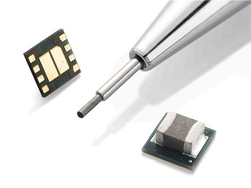
LMZ21701 SIL0008_PENCIL.gifFigure 12. LMZ21701 in the SIL0008E Package
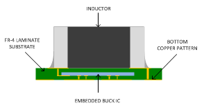
LMZ21701 SIL0008_CONSTRUCTION2.gifFigure 13. LMZ21701 Package Construction Cross Section
(Illustration Only, Not to Scale)