ZHCS572H May   2011  – October 2023 LMZ10501

PRODUCTION DATA  

  1.   1
  2. 特性
  3. 应用
  4. 说明
  5. Revision History
  6. Pin Configuration and Functions
  7. Specifications
    1. 6.1 Absolute Maximum Ratings
    2. 6.2 ESD Ratings
    3. 6.3 Recommended Operating Conditions
    4. 6.4 Thermal Information
    5. 6.5 Electrical Characteristics
    6. 6.6 System Characteristics
    7. 6.7 Typical Characteristics
  8. Detailed Description
    1. 7.1 Overview
    2. 7.2 Functional Block Diagram
    3. 7.3 Feature Description
      1. 7.3.1 Current Limit
      2. 7.3.2 Startup Behavior and Soft Start
      3. 7.3.3 Output Short Circuit Protection
      4. 7.3.4 Thermal Overload Protection
    4. 7.4 Device Functional Modes
      1. 7.4.1 Circuit Operation
      2. 7.4.2 Input Under Voltage Detection
      3. 7.4.3 Shutdown Mode
      4. 7.4.4 EN Pin Operation
      5. 7.4.5 Internal Synchronous Rectification
      6. 7.4.6 High Duty Cycle Operation
  9. Application and Implementation
    1. 8.1 Application Information
    2. 8.2 Typical Application
      1. 8.2.1 Design Requirements
      2. 8.2.2 Detailed Design Procedure
        1. 8.2.2.1 Custom Design With WEBENCH® Tools
        2. 8.2.2.2 Setting The Output Voltage
          1. 8.2.2.2.1 RT And RB Selection For Fixed VOUT
          2. 8.2.2.2.2 Output Voltage Accuracy Optimization
        3. 8.2.2.3 Dynamic Output Voltage Scaling
        4. 8.2.2.4 Integrated Inductor
        5. 8.2.2.5 Input And Output Capacitor Selection
      3. 8.2.3 Application Curves
        1. 8.2.3.1 VOUT = 1.2 V
        2. 8.2.3.2 VOUT = 1.8 V
        3. 8.2.3.3 VOUT = 2.5 V
        4. 8.2.3.4 VOUT = 3.3 V
    3. 8.3 Power Supply Recommendations
      1. 8.3.1 Voltage Range
      2. 8.3.2 Current Capability
      3. 8.3.3 Input Connection
        1. 8.3.3.1 Voltage Drops
        2. 8.3.3.2 Stability
    4. 8.4 Layout
      1. 8.4.1 Layout Guidelines
      2. 8.4.2 Layout Example
      3. 8.4.3 Package Considerations
  10. Device and Documentation Support
    1. 9.1 Device Support
      1. 9.1.1 Custom Design With WEBENCH® Tools
    2. 9.2 Documentation Support
      1. 9.2.1 Related Documentation
    3. 9.3 接收文档更新通知
    4. 9.4 支持资源
    5. 9.5 Trademarks
    6. 9.6 静电放电警告
    7. 9.7 术语表
  11. 10Mechanical, Packaging, and Orderable Information

封装选项

请参考 PDF 数据表获取器件具体的封装图。

机械数据 (封装 | 引脚)
  • SIL|8
散热焊盘机械数据 (封装 | 引脚)
订购信息

Typical Characteristics

Unless otherwise specified the following conditions apply: VIN = 3.6 V, TA = 25°C
GUID-9041F9B8-65F9-429B-ADA9-BAD30282BD3D-low.png
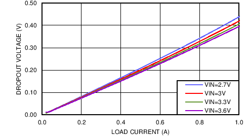
Figure 6-1 Dropout Voltage vs Load Current and Input Voltage, TA = 85°C
GUID-A56E753C-A08B-464E-B31D-618D96153780-low.png
Figure 6-3 Thermal Derating VOUT = 1.8 V, ΘJA = 77°C/W
GUID-673BE2B3-358D-4E2F-9A78-101051C8658D-low.png
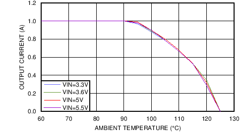
Figure 6-5 Thermal Derating VOUT = 3.3 V, ΘJA = 77°C/W
GUID-F5B621A2-3680-4EF3-A838-99EAEC8BA9F8-low.png
Figure 6-7 Conducted EMI VIN = 5.0 V, VOUT = 1.8 V, IOUT = 1-A Default Evaluation Board BOM with Additional 2.2-µh 1-µf LC Input Filter
GUID-E7A9831E-DA43-4761-BD0B-B4B8E34B4CF7-low.png
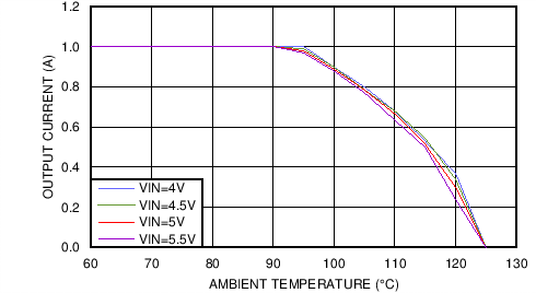
Figure 6-2 Thermal Derating VOUT = 1.2 V, ΘJA = 77°C/W
GUID-478C4945-FDEA-464C-A4FC-FAB632AB9963-low.png
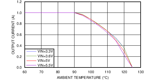
Figure 6-4 Thermal Derating VOUT = 2.5 V, ΘJA = 77°C/W
GUID-8551EDDD-D3CC-41E0-895A-FD2A45C498FA-low.png
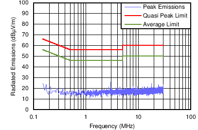
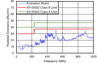
Figure 6-6 Radiated EMI (Cispr22) VIN = 5 V, VOUT = 1.8 V, IOUT = 1-A Default Evaluation Board BOM
GUID-9F2E431F-4BBB-4196-A1F1-E56DCDFE0556-low.gif
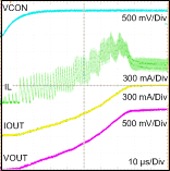
Figure 6-8 Startup