ZHCSJO3B May 2019 – November 2020 LMR34215-Q1
PRODUCTION DATA
- 1 特性
- 2 应用
- 3 说明
- 4 Revision History
- 5 Device Comparison Table
- 6 Pin Configuration and Functions
- 7 Specifications
- 8 Detailed Description
- 9 Power Supply Recommendations
- 10Layout
- 11Device and Documentation Support
- 12Mechanical, Packaging, and Orderable Information
8.1 Overview
The LMR34215-Q1 is a synchronous peak-current-mode buck regulator designed for a wide variety of applications. The regulator automatically switches modes between PFM and PWM, depending on load. At heavy loads, the device operates in PWM at a constant switching frequency. At light loads, the mode changes to PFMW with diode emulation allowing DCM. This reduces the input supply current and keeps efficiency high. The device features internal loop compensation which reduces design time and requires fewer external components than externally compensated regulators.
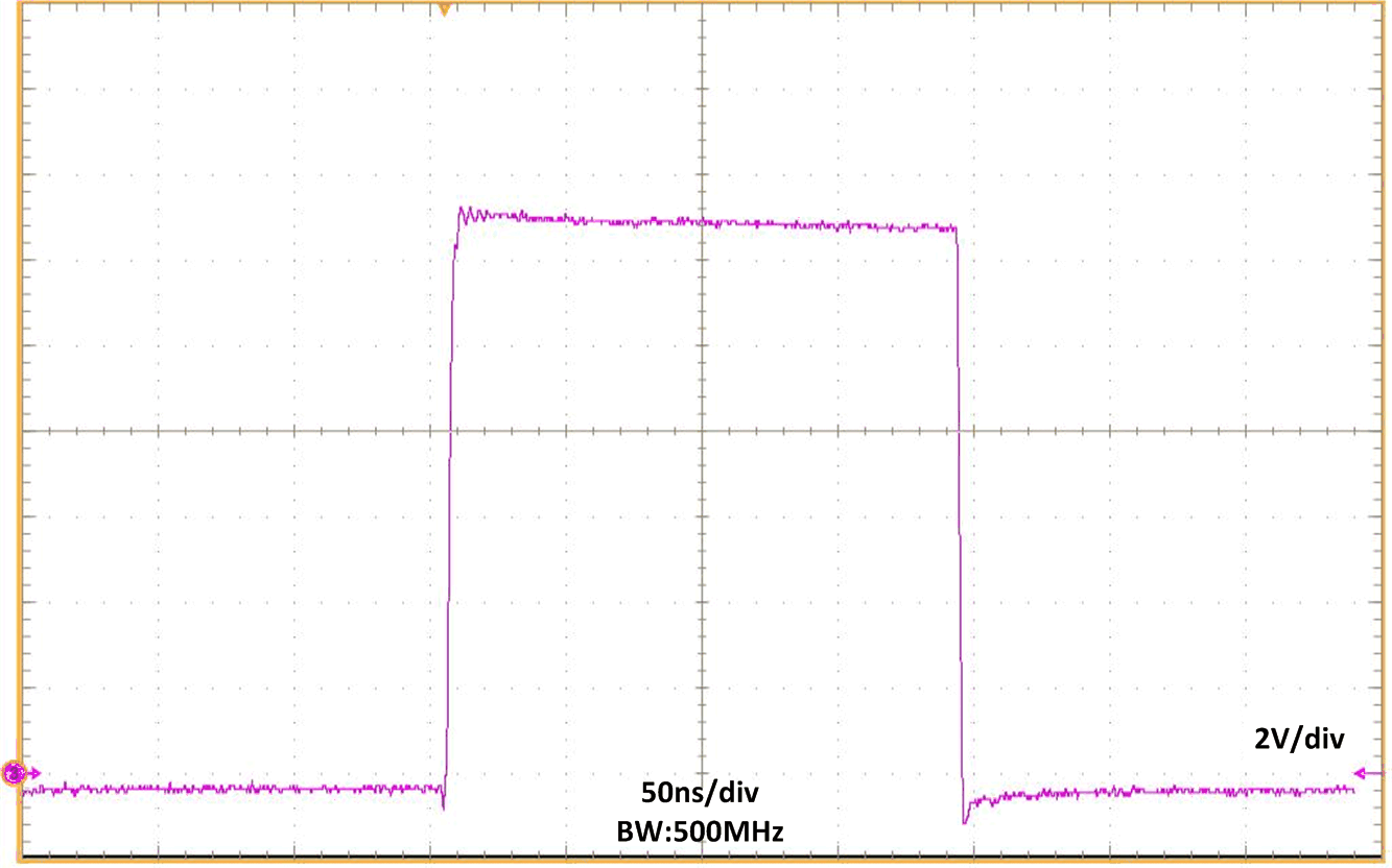
The LMR34215-Q1 is designed with a flip-chip or HotRod technology, greatly reducing the parasitic inductance of pins. In addition, the layout of the device allows for reduction in the radiated noise generated by the switching action through partial cancellation of the current generated magnetic field. As a result, the switch-node waveform exhibits less overshoot and ringing.
 Figure 8-1 Switch Node Waveform