ZHCSF95C December 2015 – February 2018 LMR23610
PRODUCTION DATA.
- 1 特性
- 2 应用
- 3 说明
- 4 修订历史记录
- 5 Pin Configuration and Functions
- 6 Specifications
-
7 Detailed Description
- 7.1 Overview
- 7.2 Functional Block Diagram
- 7.3
Feature Description
- 7.3.1 Fixed Frequency Peak Current Mode Control
- 7.3.2 Adjustable Output Voltage
- 7.3.3 EN/SYNC
- 7.3.4 VCC, UVLO
- 7.3.5 Minimum ON-Time, Minimum OFF-Time and Frequency Foldback at Dropout Conditions
- 7.3.6 Internal Compensation and CFF
- 7.3.7 Bootstrap Voltage (BOOT)
- 7.3.8 Overcurrent and Short-Circuit Protection
- 7.3.9 Thermal Shutdown
- 7.4 Device Functional Modes
-
8 Application and Implementation
- 8.1 Application Information
- 8.2
Typical Applications
- 8.2.1 Design Requirements
- 8.2.2
Detailed Design Procedure
- 8.2.2.1 Custom Design With WEBENCH® Tools
- 8.2.2.2 Output Voltage Setpoint
- 8.2.2.3 Switching Frequency
- 8.2.2.4 Inductor Selection
- 8.2.2.5 Output Capacitor Selection
- 8.2.2.6 Feed-Forward Capacitor
- 8.2.2.7 Input Capacitor Selection
- 8.2.2.8 Bootstrap Capacitor Selection
- 8.2.2.9 VCC Capacitor Selection
- 8.2.2.10 Undervoltage Lockout Setpoint
- 8.2.3 Application Curves
- 9 Power Supply Recommendations
- 10Layout
- 11器件和文档支持
- 12机械、封装和可订购信息
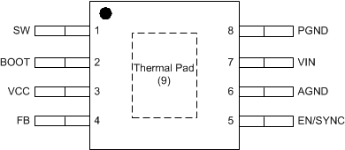
5 Pin Configuration and Functions
DDA Package
8-Pin HSOIC
Top View

Pin Functions
| PIN | I/O(1) | DESCRIPTION | |
|---|---|---|---|
| NO. | NAME | ||
| 1 | SW | O | Switching output of the regulator. Internally connected to both power MOSFETs. Connect to power inductor. |
| 2 | BOOT | O | Boot-strap capacitor connection for high-side driver. Connect a high-quality 470-nF capacitor from BOOT to SW. |
| 3 | VCC | O | Internal bias supply output for bypassing. Connect a 2.2-µF, 16-V bypass capacitor from this pin to AGND. Do not connect external loading to this pin. Never short this pin to ground during operation. |
| 4 | FB | I | Feedback input to regulator, connect the feedback resistor divider tap to this pin. |
| 5 | EN/SYNC | I | Enable input to regulator. High = On, Low = Off. Can be connected to VIN. Do not float. Adjust the input under voltage lockout with two resistors. The internal oscillator can be synchronized to an external clock by coupling a positive pulse into this pin through a small coupling capacitor. See EN/SYNC for details. |
| 6 | AGND | G | Analog ground pin. Ground reference for internal references and logic. Connect to system ground. |
| 7 | VIN | I | Input supply voltage. |
| 8 | PGND | G | Power ground pin, connected internally to the low side power FET. Connect to system ground, PAD, AGND, ground pins of CIN and COUT. Path to CIN must be as short as possible. |
| 9 | PAD | G | Low impedance connection to AGND. Connect to PGND on PCB. Major heat dissipation path of the die. Must be used for heat sinking to ground plane on PCB. |
(1) I = Input, O = Output, G = Ground