SNOSA71L October 2004 – September 2015 LMP2011 , LMP2012
PRODUCTION DATA.
- 1 Features
- 2 Applications
- 3 Description
- 4 Revision History
- 5 Pin Configuration and Functions
-
6 Specifications
- 6.1 Absolute Maximum Ratings
- 6.2 ESD Ratings
- 6.3 Recommended Operating Conditions
- 6.4 Thermal Information: LMP2011
- 6.5 Thermal Information: LMP2012
- 6.6 2.7-V DC Electrical Characteristics
- 6.7 2.7-V AC Electrical Characteristics
- 6.8 5-V DC Electrical Characteristics
- 6.9 5-V AC Electrical Characteristics
- 6.10 Typical Characteristics
- 7 Detailed Description
- 8 Application and Implementation
- 9 Power Supply Recommendations
- 10Layout
- 11Device and Documentation Support
- 12Mechanical, Packaging, and Orderable Information
封装选项
机械数据 (封装 | 引脚)
散热焊盘机械数据 (封装 | 引脚)
- DGK|8
订购信息
6 Specifications
6.1 Absolute Maximum Ratings
See (1)(2)| MIN | MAX | UNIT | ||
|---|---|---|---|---|
| Supply Voltage | 5.8 | V | ||
| Common-Mode Input Voltage | (V-) - 0.3 | (V+) + 0.3 | V | |
| Lead Temperature (soldering 10 sec.) | 300 | °C | ||
| Differential Input Voltage | ±Supply Voltage | |||
| Current at Input Pin | 30 | 30 | mA | |
| Current at Output Pin | 30 | 30 | mA | |
| Current at Power Supply Pin | 50 | 30 | mA | |
| Storage Temperature | −65 | 150 | °C | |
(1) Absolute Maximum Ratings indicate limits beyond which damage may occur. Operating Ratings indicate conditions for which the device is intended to be functional, but specific performance is not ensured. For ensured specifications and test conditions, see the Electrical Characteristics.
(2) If Military/Aerospace specified devices are required, please contact the Texas Instruments Sales Office/ Distributors for availability and specifications.
6.2 ESD Ratings
| VALUE | UNIT | |||
|---|---|---|---|---|
| V(ESD) | Electrostatic discharge | Human body model (HBM), per ANSI/ESDA/JEDEC JS-001(1) | ±2000 | V |
| Machine model | ±200 | |||
(1) JEDEC document JEP155 states that 500-V HBM allows safe manufacturing with a standard ESD control process.
6.3 Recommended Operating Conditions
| MIN | MAX | UNIT | |
|---|---|---|---|
| Supply Voltage | 2.7 | 5.25 | V |
| Operating Temperature Range | −40 | 125 | °C |
6.4 Thermal Information: LMP2011
| THERMAL METRIC(1) | LMP2011 | UNIT | ||
|---|---|---|---|---|
| D (SOIC) | DBV (SOT-23) | |||
| 8 PINS | 5 PINS | |||
| RθJA | Junction-to-ambient thermal resistance | 119 | 164 | °C/W |
| RθJC(top) | Junction-to-case (top) thermal resistance | 66 | 116 | °C/W |
| RθJB | Junction-to-board thermal resistance | 60 | 28 | °C/W |
| ψJT | Junction-to-top characterization parameter | 17 | 13 | °C/W |
| ψJB | Junction-to-board characterization parameter | 59 | 27 | °C/W |
(1) For more information about traditional and new thermal metrics, see the Semiconductor and IC Package Thermal Metrics application report, SPRA953.
6.5 Thermal Information: LMP2012
| THERMAL METRIC(1) | LMP2012 | UNIT | ||
|---|---|---|---|---|
| D (SOIC) | DGK (VSSOP) | |||
| 8 PINS | 8 PINS | |||
| RθJA | Junction-to-ambient thermal resistance | 110 | 157 | °C/W |
| RθJC(top) | Junction-to-case (top) thermal resistance | 50 | 51 | °C/W |
| RθJB | Junction-to-board thermal resistance | 52 | 77 | °C/W |
| ψJT | Junction-to-top characterization parameter | 8 | 5 | °C/W |
| ψJB | Junction-to-board characterization parameter | 51 | 75 | °C/W |
(1) For more information about traditional and new thermal metrics, see the Semiconductor and IC Package Thermal Metrics application report, SPRA953.
6.6 2.7-V DC Electrical Characteristics
Unless otherwise specified, all limits ensured for TJ = 25°C, V+ = 2.7 V, V− = 0 V, V CM = 1.35 V, VO = 1.35 V, and RL > 1 MΩ.| PARAMETER | TEST CONDITIONS | MIN(2) | TYP(1) | MAX(2) | UNIT | ||
|---|---|---|---|---|---|---|---|
| VOS | Input Offset Voltage (LMP2011 only) |
TJ = 25°C | 0.8 | 25 | μV | ||
| The temperature extremes | 60 | ||||||
| Input Offset Voltage (LMP2012 only) |
TJ = 25°C | 0.8 | 36 | ||||
| The temperature extremes | 60 | ||||||
| Offset Calibration Time | TJ = 25°C | 0.5 | 10 | ms | |||
| The temperature extremes | 12 | ||||||
| TCVOS | Input Offset Voltage | 0.015 | μV/°C | ||||
| Long-Term Offset Drift | 0.006 | μV/month | |||||
| Lifetime VOS Drift | 2.5 | μV | |||||
| IIN | Input Current | -3 | pA | ||||
| IOS | Input Offset Current | 6 | pA | ||||
| RIND | Input Differential Resistance | 9 | MΩ | ||||
| CMRR | Common Mode Rejection Ratio | −0.3 ≤ VCM ≤ 0.9 V, 0 ≤ VCM ≤ 0.9 V |
TJ = 25°C | 95 | 130 | dB | |
| The temperature extremes | 90 | ||||||
| PSRR | Power Supply Rejection Ratio | TJ = 25°C | 95 | 120 | dB | ||
| The temperature extremes | 90 | ||||||
| AVOL | Open Loop Voltage Gain | RL = 10 kΩ | TJ = 25°C | 95 | 130 | dB | |
| The temperature extremes | 90 | ||||||
| RL = 2 kΩ | TJ = 25°C | 90 | 124 | ||||
| The temperature extremes | 85 | ||||||
| VO | Output Swing (LMP2011 only) |
RL = 10 kΩ to 1.35 V, VIN(diff) = ±0.5 V |
TJ = 25°C | 2.665 | 2.68 | V | |
| The temperature extremes | 2.655 | ||||||
| TJ = 25°C | 0.033 | 0.060 | |||||
| The temperature extremes | 0.075 | ||||||
| RL = 2 kΩ to 1.35 V, VIN(diff) = ±0.5 V |
TJ = 25°C | 2.630 | 2.65 | V | |||
| The temperature extremes | 2.615 | ||||||
| TJ = 25°C | 0.061 | 0.085 | |||||
| The temperature extremes | 0.105 | ||||||
| Output Swing (LMP2012 only) |
RL = 10 kΩ to 1.35 V, VIN(diff) = ±0.5 V |
TJ = 25°C | 2.64 | 2.68 | V | ||
| The temperature extremes | 2.63 | ||||||
| TJ = 25°C | 0.033 | 0.060 | |||||
| The temperature extremes | 0.075 | ||||||
| RL = 2 kΩ to 1.35 V, VIN(diff) = ±0.5 V |
TJ = 25°C | 2.615 | 2.65 | V | |||
| The temperature extremes | 2.6 | ||||||
| TJ = 25°C | 0.061 | 0.085 | |||||
| The temperature extremes | 0.105 | ||||||
| IO | Output Current | Sourcing, VO = 0 V, VIN(diff) = ±0.5 V |
TJ = 25°C | 5 | 12 | mA | |
| The temperature extremes | 3 | ||||||
| VIN(diff) = ±0.5 V, Sinking, VO = 5 V |
TJ = 25°C | 5 | 18 | ||||
| The temperature extremes | 3 | ||||||
| IS | Supply Current per Channel | TJ = 25°C | 0.919 | 1.20 | mA | ||
| The temperature extremes | 1.50 | ||||||
(1) Typical values represent the most likely parametric norm.
(2) Limits are 100% production tested at 25°C. Limits over the operating temperature range are ensured through correlations using statistical quality control (SQC) method.
6.7 2.7-V AC Electrical Characteristics
TJ = 25°C, V+ = 2.7 V, V− = 0 V, VCM = 1.35 V, VO = 1.35 V, and RL > 1 MΩ.| PARAMETER | TEST CONDITIONS | MIN(2) | TYP(1) | MAX(2) | UNIT | ||
|---|---|---|---|---|---|---|---|
| GBW | Gain-Bandwidth Product | 3 | MHz | ||||
| SR | Slew Rate | 4 | V/μs | ||||
| θ m | Phase Margin | 60 | Deg | ||||
| Gm | Gain Margin | −14 | dB | ||||
| en | Input-Referred Voltage Noise | 35 | nV/√Hz | ||||
| enp-p | Input-Referred Voltage Noise | RS = 100 Ω, DC to 10 Hz | 850 | nVpp | |||
| trec | Input Overload Recovery Time | 50 | ms | ||||
(1) Typical values represent the most likely parametric norm.
(2) Limits are 100% production tested at 25°C. Limits over the operating temperature range are ensured through correlations using statistical quality control (SQC) method.
6.8 5-V DC Electrical Characteristics
Unless otherwise specified, all limits ensured for TJ = 25°C, V+ = 5 V, V− = 0 V, V CM = 2.5 V, VO = 2.5 V, and RL > 1MΩ.| PARAMETER | TEST CONDITIONS | MIN(2) | TYP(1) | MAX(2) | UNIT | ||
|---|---|---|---|---|---|---|---|
| VOS | Input Offset Voltage (LMP2011 only) |
TJ = 25°C | 0.12 | 25 | μV | ||
| The temperature extremes | 60 | ||||||
| Input Offset Voltage (LMP2012 only) |
TJ = 25°C | 0.12 | 36 | ||||
| The temperature extremes | 60 | ||||||
| Offset Calibration Time | TJ = 25°C | 0.5 | 10 | ms | |||
| The temperature extremes | 12 | ||||||
| TCVOS | Input Offset Voltage | 0.015 | μV/°C | ||||
| Long-Term Offset Drift | 0.006 | μV/month | |||||
| Lifetime VOS Drift | 2.5 | μV | |||||
| IIN | Input Current | -3 | pA | ||||
| IOS | Input Offset Current | 6 | pA | ||||
| RIND | Input Differential Resistance | 9 | MΩ | ||||
| CMRR | Common Mode Rejection Ratio | −0.3 ≤ VCM ≤ 3.2, 0 ≤ VCM ≤ 3.2 |
TJ = 25°C | 100 | 130 | dB | |
| The temperature extremes | 90 | ||||||
| PSRR | Power Supply Rejection Ratio | TJ = 25°C | 95 | 120 | dB | ||
| The temperature extremes | 90 | ||||||
| AVOL | Open Loop Voltage Gain | RL = 10 kΩ | TJ = 25°C | 105 | 130 | dB | |
| The temperature extremes | 100 | ||||||
| RL = 2 kΩ | TJ = 25°C | 95 | 132 | ||||
| The temperature extremes | 90 | ||||||
| VO | Output Swing (LMP2011 only) |
RL = 10 kΩ to 2.5 V, VIN(diff) = ±0.5 V |
TJ = 25°C | 4.96 | 4.978 | V | |
| The temperature extremes | 4.95 | ||||||
| TJ = 25°C | 0.040 | 0.070 | |||||
| The temperature extremes | 0.085 | ||||||
| RL = 2 kΩ to 2.5 V, VIN(diff) = ±0.5 V |
TJ = 25°C | 4.895 | 4.919 | V | |||
| The temperature extremes | 4.875 | ||||||
| TJ = 25°C | 0.091 | 0.115 | |||||
| The temperature extremes | 0.140 | ||||||
| Output Swing (LMP2012 only) |
RL = 10 kΩ to 2.5 V, VIN(diff) = ±0.5 V |
TJ = 25°C | 4.92 | 4.978 | V | ||
| The temperature extremes | 4.91 | ||||||
| TJ = 25°C | 0.040 | 0.080 | |||||
| The temperature extremes | 0.095 | ||||||
| RL = 2 kΩ to 2.5 V, VIN(diff) = ±0.5 V |
TJ = 25°C | 4.875 | 4.919 | V | |||
| The temperature extremes | 4.855 | ||||||
| TJ = 25°C | 0.0.91 | 0.125 | |||||
| The temperature extremes | 0.150 | ||||||
| IO | Output Current | Sourcing, VO = 0 V, VIN(diff) = ±0.5 V |
TJ = 25°C | 8 | 15 | mA | |
| The temperature extremes | 6 | ||||||
| Sinking, VO = 5 V, VIN(diff) = ±0.5 V |
TJ = 25°C | 8 | 17 | ||||
| The temperature extremes | 6 | ||||||
| IS | Supply Current per Channel | TJ = 25°C | 0.930 | 1.20 | mA | ||
| The temperature extremes | 1.50 | ||||||
(1) Typical values represent the most likely parametric norm.
(2) Limits are 100% production tested at 25°C. Limits over the operating temperature range are ensured through correlations using statistical quality control (SQC) method.
6.9 5-V AC Electrical Characteristics
TJ = 25°C, V+ = 5 V, V− = 0 V, VCM = 2.5 V, VO = 2.5 V, and RL > 1MΩ.| PARAMETER | TEST CONDITIONS | MIN(2) | TYP(1) | MAX(2) | UNIT | ||
|---|---|---|---|---|---|---|---|
| GBW | Gain-Bandwidth Product | 3 | MHz | ||||
| SR | Slew Rate | 4 | V/μs | ||||
| θ m | Phase Margin | 60 | deg | ||||
| Gm | Gain Margin | −15 | dB | ||||
| en | Input-Referred Voltage Noise | 35 | nV/√Hz | ||||
| enp-p | Input-Referred Voltage Noise | RS = 100 Ω, DC to 10 Hz | 850 | nVpp | |||
| trec | Input Overload Recovery Time | 50 | ms | ||||
(1) Typical values represent the most likely parametric norm.
(2) Limits are 100% production tested at 25°C. Limits over the operating temperature range are ensured through correlations using statistical quality control (SQC) method.
6.10 Typical Characteristics
TA=25C, VS= 5 V unless otherwise specified.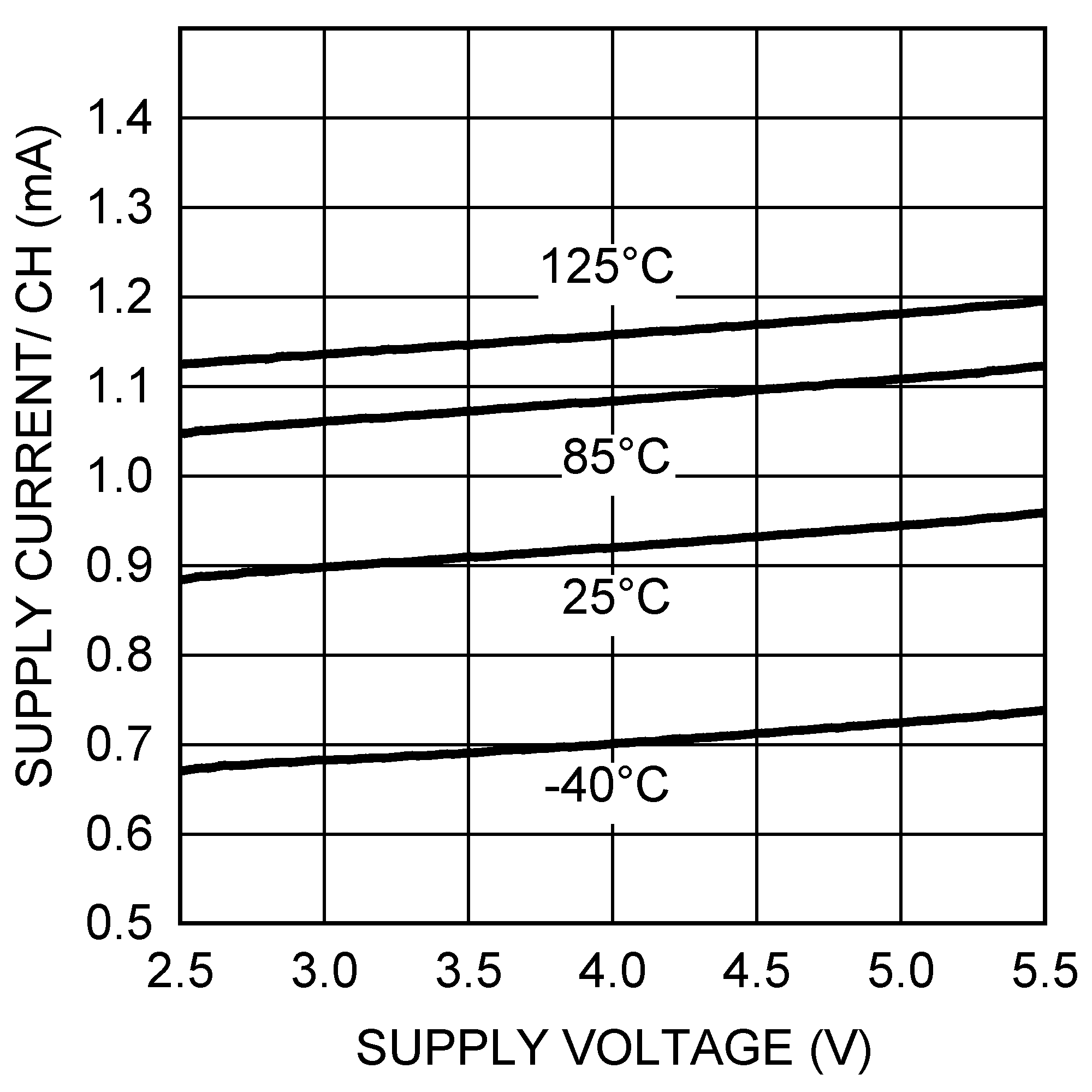 Figure 1. Supply Current vs Supply Voltage
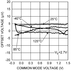 Figure 3. Offset Voltage vs Common Mode
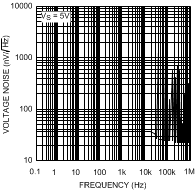 Figure 5. Voltage Noise vs Frequency
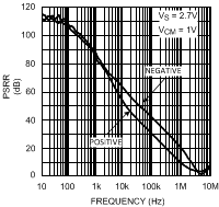 Figure 7. PSRR vs Frequency
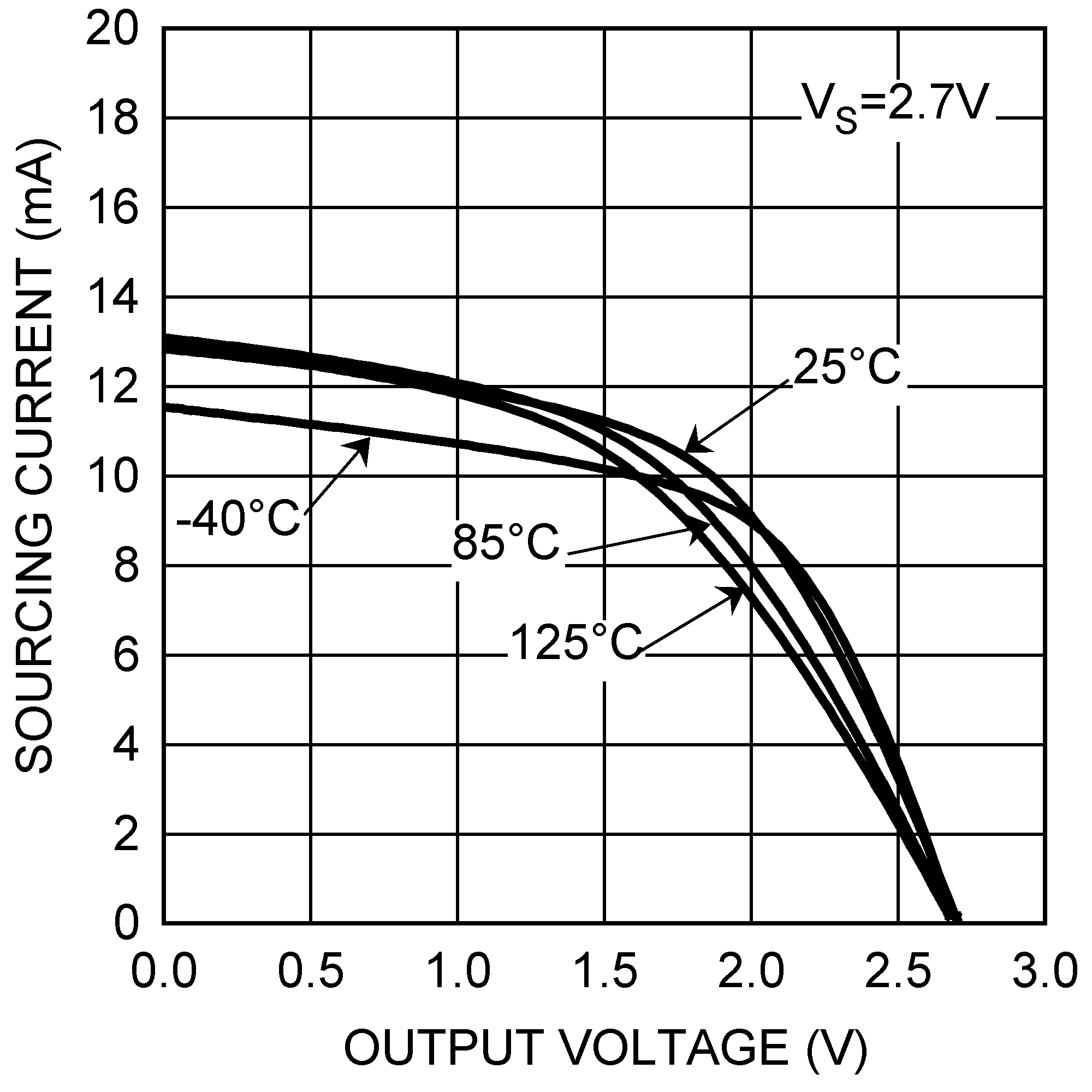 Figure 9. Output Sourcing at 2.7 V
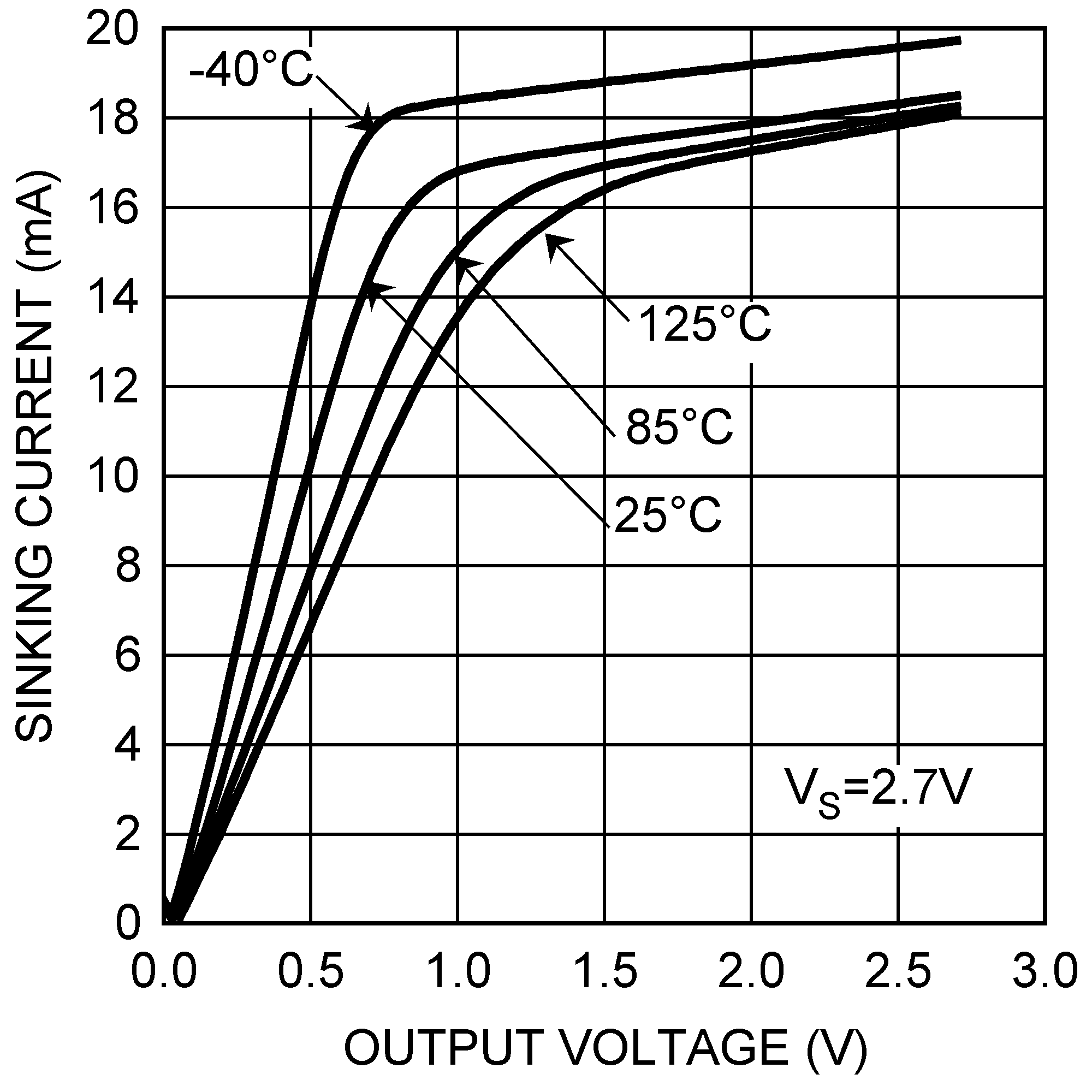 Figure 11. Output Sinking at 2.7 V
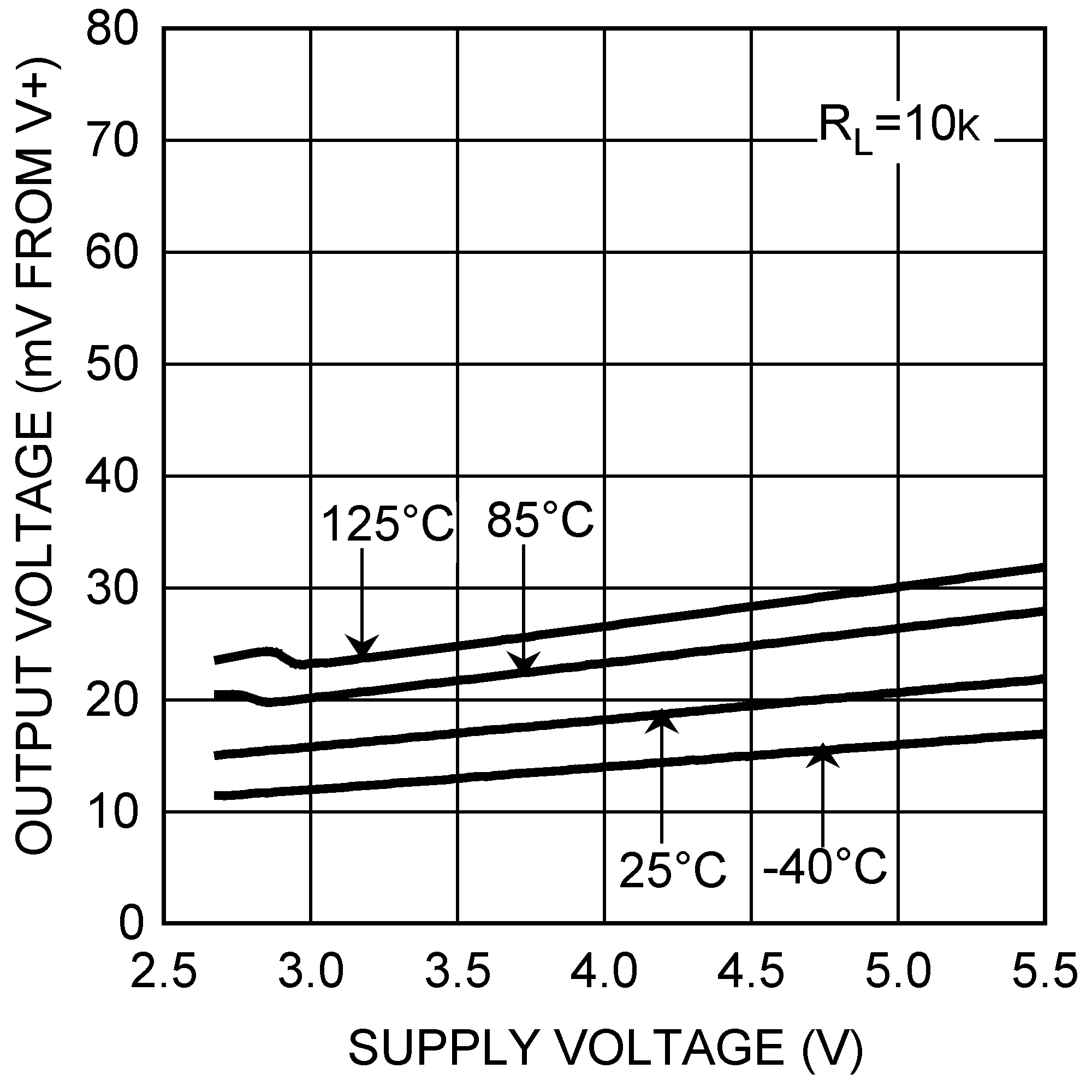 Figure 13. Maximum Output Swing vs Supply Voltage
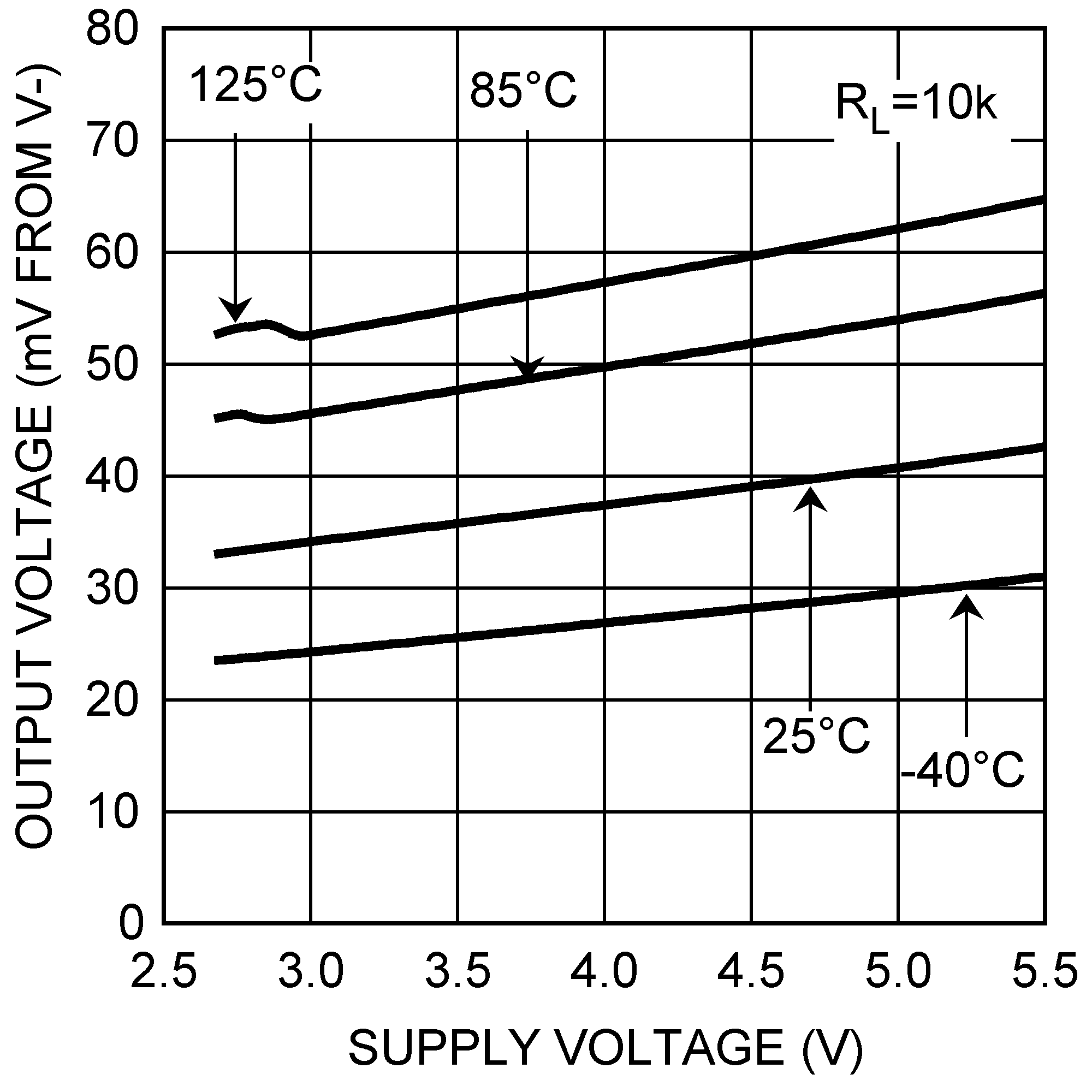 Figure 15. Minimum Output Swing vs Supply Voltage
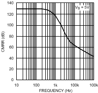 Figure 17. CMRR vs Frequency
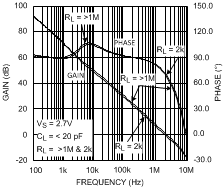 Figure 19. Open Loop Gain and Phase vs RL at 2.7 V
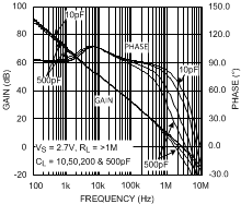 Figure 21. Open Loop Gain and Phase vs CL at 2.7 V
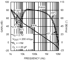 Figure 23. Open Loop Gain and Phase vs Temperature
at 2.7 V
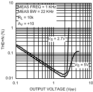 Figure 25. THD+N vs AMPL
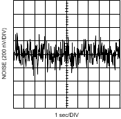 Figure 27. 0.1 Hz − 10 Hz Noise vs Time
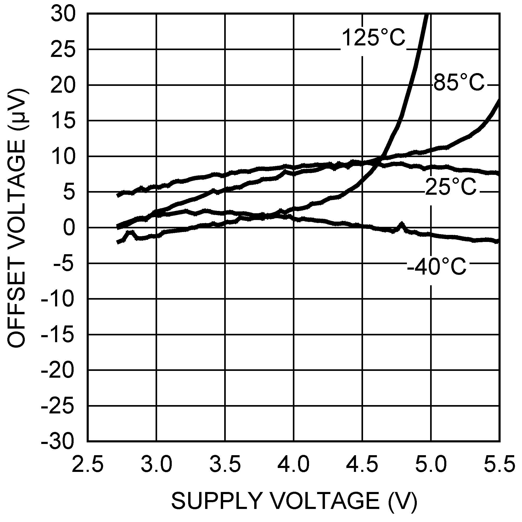 Figure 2. Offset Voltage vs Supply Voltage
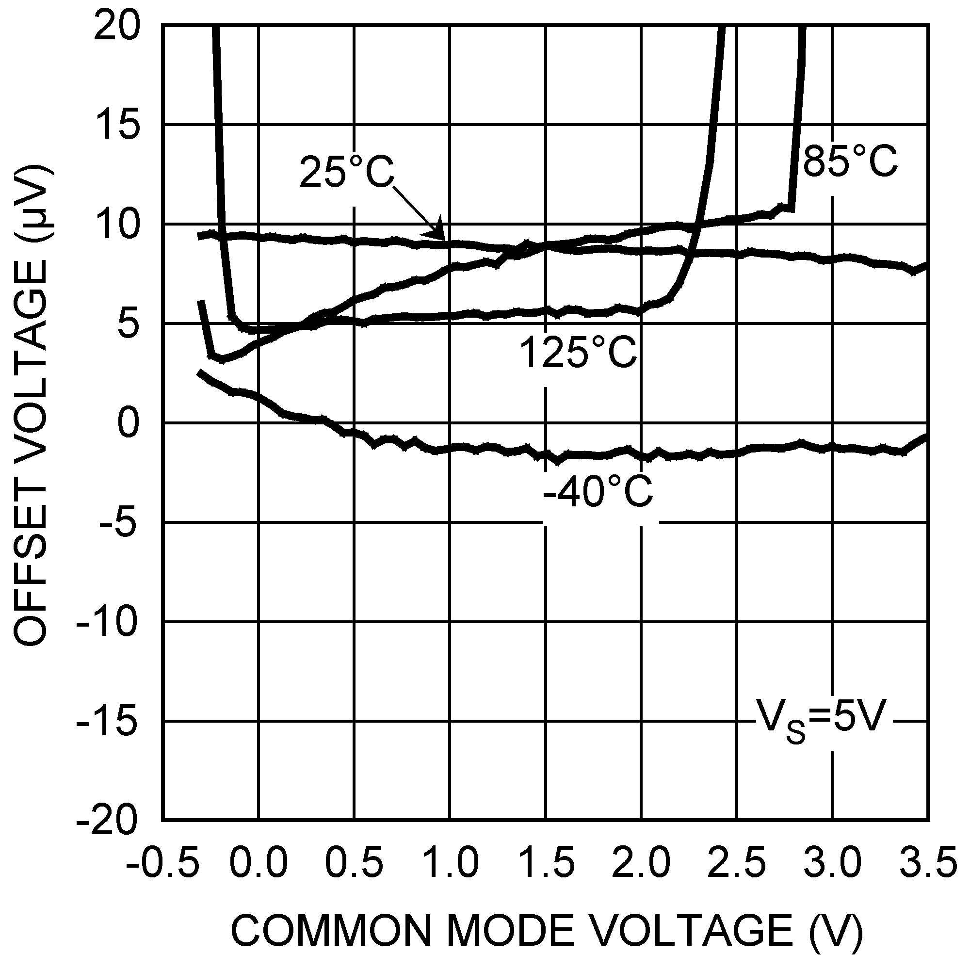 Figure 4. Offset Voltage vs Common Mode
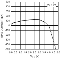 Figure 6. Input Bias Current vs Common Mode
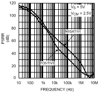 Figure 8. PSRR vs Frequency
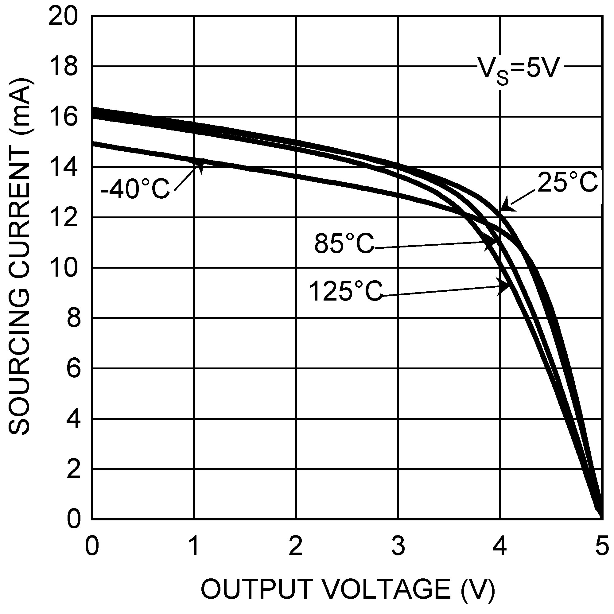 Figure 10. Output Sourcing at 5 V
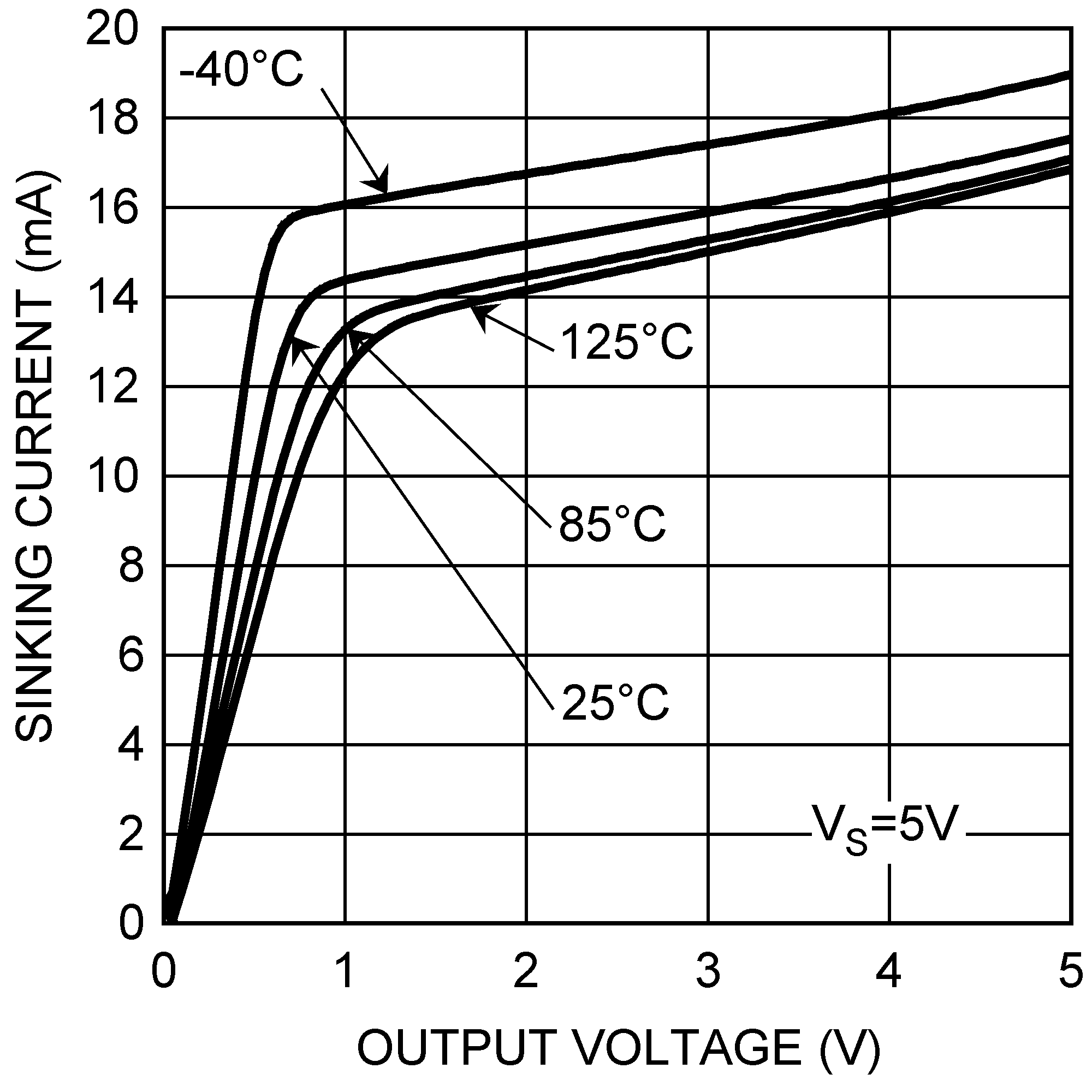 Figure 12. Output Sinking at 5 V
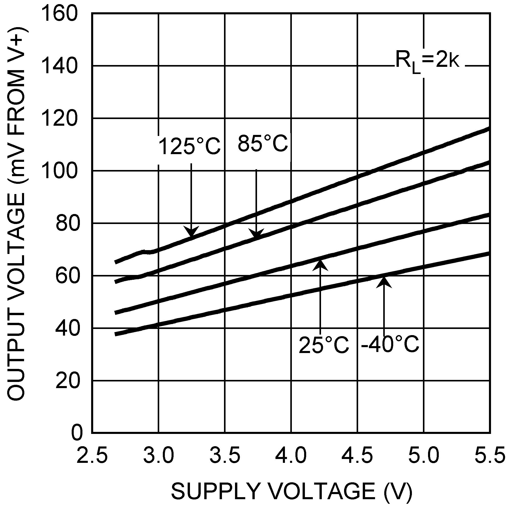 Figure 14. Maximum Output Swing vs Supply Voltage
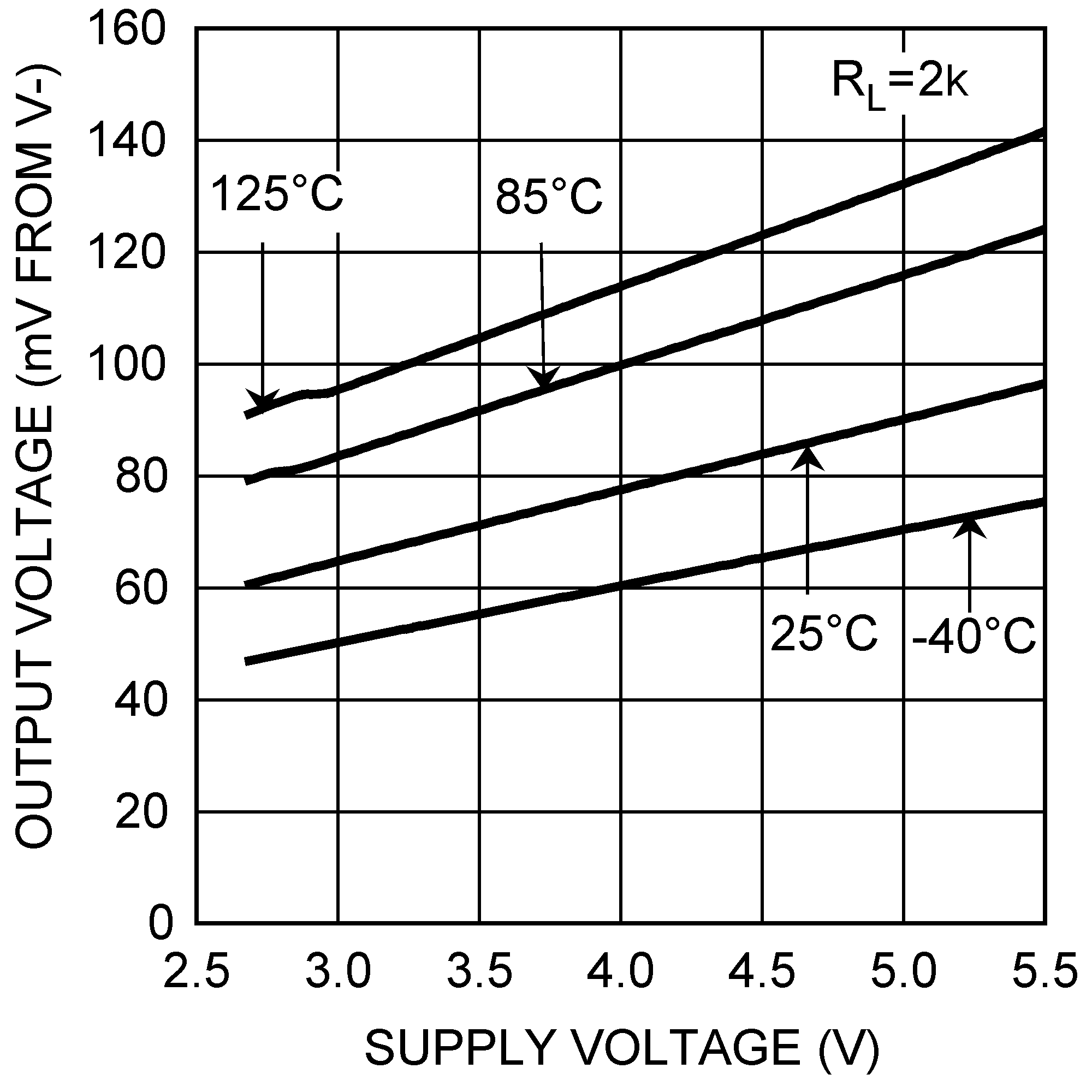 Figure 16. Minimum Output Swing vs Supply Voltage
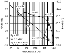 Figure 18. Open Loop Gain and Phase vs Supply Voltage
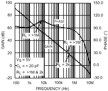 Figure 20. Open Loop Gain and Phase vs RL at 5 V
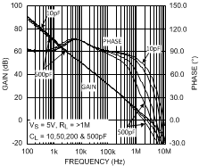 Figure 22. Open Loop Gain and Phase vs CL at 5 V
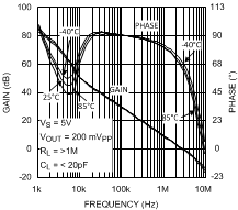 Figure 24. Open Loop Gain and Phase vs Temperature
at 5 V
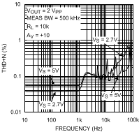 Figure 26. THD+N vs Frequency