SNOSA71L October 2004 – September 2015 LMP2011 , LMP2012
PRODUCTION DATA.
- 1 Features
- 2 Applications
- 3 Description
- 4 Revision History
- 5 Pin Configuration and Functions
-
6 Specifications
- 6.1 Absolute Maximum Ratings
- 6.2 ESD Ratings
- 6.3 Recommended Operating Conditions
- 6.4 Thermal Information: LMP2011
- 6.5 Thermal Information: LMP2012
- 6.6 2.7-V DC Electrical Characteristics
- 6.7 2.7-V AC Electrical Characteristics
- 6.8 5-V DC Electrical Characteristics
- 6.9 5-V AC Electrical Characteristics
- 6.10 Typical Characteristics
- 7 Detailed Description
- 8 Application and Implementation
- 9 Power Supply Recommendations
- 10Layout
- 11Device and Documentation Support
- 12Mechanical, Packaging, and Orderable Information
封装选项
机械数据 (封装 | 引脚)
散热焊盘机械数据 (封装 | 引脚)
- DGK|8
订购信息
7 Detailed Description
7.1 Overview
The LMP201x series offers unprecedented accuracy and stability in space-saving miniature packaging while also being offered at an affordable price. This device utilizes patented techniques to measure and continually correct the input offset error voltage. The result is an amplifier which is ultra stable over time and temperature.
7.2 Functional Block Diagram

7.3 Feature Description
7.3.1 How the LMP201x Works
The LMP201x uses new, patented auto-zero techniques to achieve the high DC accuracy traditionally associated with chopper-stabilized amplifiers without the major drawbacks produced by chopping. The LMP201x continuously monitors the input offset and corrects this error.
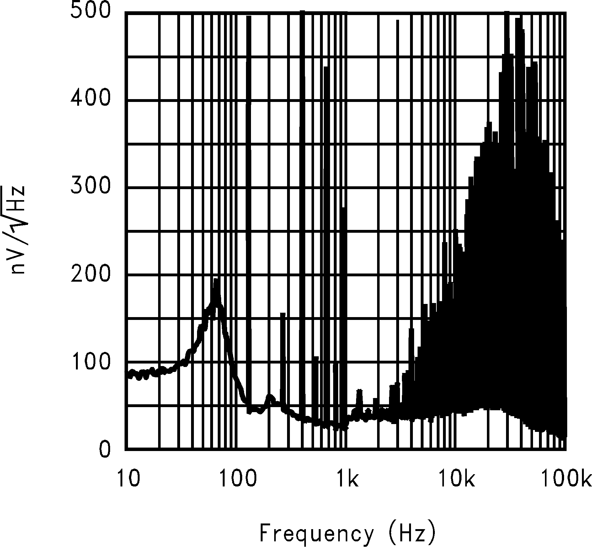
The conventional low-frequency chopping process produces many mixing products, both sums and differences, between the chopping frequency and the incoming signal frequency. This mixing causes large amounts of distortion, particularly when the signal frequency approaches the chopping frequency. Even without an incoming signal, the chopper harmonics mix with each other to produce even more trash. If this sounds unlikely or difficult to understand, look at the plot (Figure 28), of the output of a typical (MAX432) chopper-stabilized op amp. This is the output when there is no incoming signal, just the amplifier in a gain of -10 with the input grounded. The chopper is operating at about 150 Hz; the rest is mixing products. Add an input signal and the noise gets much worse.
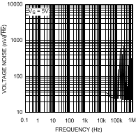
Compare this plot with Figure 29 of the LMP201x. This data was taken under the exact same conditions. The auto-zero action is visible at about 30 kHz but note the absence of mixing products at other frequencies. As a result, the LMP201x has very low distortion of 0.02% and very low mixing products.
 Figure 28. The Output of a Chopper Stabilized Op Amp (MAX432)
 Figure 29. The Output of the LMP2011/LMP2012
7.3.2 The Benefits of LMP201x: No 1/F Noise
Using patented methods, the LMP201x eliminates the 1/f noise present in other amplifiers. This noise, which increases as frequency decreases, is a major source of measurement error in all DC-coupled measurements. Low-frequency noise appears as a constantly-changing signal in series with any measurement being made. As a result, even when the measurement is made rapidly, this constantly-changing noise signal will corrupt the result.
The value of this noise signal can be surprisingly large. For example: If a conventional amplifier has a flat-band noise level of 10 nV/√Hz and a noise corner of 10 Hz, the RMS noise at 0.001 Hz is 1 µV/√Hz. This is equivalent to a 0.50-µV peak-to-peak error, in the frequency range 0.001 Hz to 1.0 Hz. In a circuit with a gain of 1000, this produces a 0.50-mV peak-to-peak output error. This number of 0.001 Hz might appear unreasonably low, but when a data acquisition system is operating for 17 minutes, it has been on long enough to include this error. In this same time, the LMP201x will only have a 0.21-mV output error. This is smaller by 2.4×. This 1/f error gets even larger at lower frequencies. At the extreme, many people try to reduce this error by integrating or taking several samples of the same signal. This is also doomed to failure because the 1/f nature of this noise means that taking longer samples just moves the measurement into lower frequencies where the noise level is even higher.
The LMP201x eliminates this source of error. The noise level is constant with frequency so that reducing the bandwidth reduces the errors caused by noise.
7.3.3 No External Capacitors Required
The LMP201x does not need external capacitors. This eliminates the problems caused by capacitor leakage and dielectric absorption, which can cause delays of several seconds from turn-on until the amplifier's error has settled.
7.3.4 Copper Leadframe
Another source of error that is rarely mentioned is the error voltage caused by the inadvertent thermocouples created when the common Kovar type IC package lead materials are soldered to a copper printed circuit board. These steel-based leadframe materials can produce over 35 μV/°C when soldered onto a copper trace. This can result in thermocouple noise that is equal to the LMP201x noise when there is a temperature difference of only 0.0014°C between the lead and the board!
For this reason, the lead-frame of the LMP201x is made of copper. This results in equal and opposite junctions which cancel this effect. The extremely small size of the SOT-23 package results in the leads being very close together. This further reduces the probability of temperature differences and hence decreases thermal noise.
7.3.5 More Benefits
The LMP201x offers the benefits mentioned above and more. It has a rail-to-rail output and consumes only 950 µA of supply current while providing excellent DC and AC electrical performance. In DC performance, the LMP201x achieves 130 dB of CMRR, 120 dB of PSRR, and 130 dB of open loop gain. In AC performance, the LMP201x provides 3 MHz of gain-bandwidth product and 4 V/µs of slew rate.
7.4 Device Functional Modes
7.4.1 Input Currents
The LMP201x input currents are different than standard bipolar or CMOS input currents. Due to the auto-zero action of the input stage, the input current appears as a pulsating current at the chopping frequency (35 kHz) flowing in one input and out the other. Under most operating conditions, these currents are in the picoamp level and will have little or no effect in most circuits.
These currents tend to increase slightly when the common-mode voltage is near the minus supply. (See the Typical Characteristics.) At high temperatures such as 85°C, the input currents become larger, 0.5 nA typical, and are both positive except when the VCM is near V−. If operation is expected at low common-mode voltages and high temperature, do not add resistance in series with the inputs to balance the impedances. Doing this can cause an increase in offset voltage. A small resistance such as 1 kΩ can provide some protection against very large transients or overloads, and will not increase the offset significantly.
Because of these issues, the LMV201x is not recommended for source impedances over 1MΩ.
7.4.2 Overload Recovery
The LMP201x recovers from input overload much faster than most chopper-stabilized op amps. Recovery from driving the amplifier to 2X the full scale output, only requires about 40 ms. Many chopper-stabilized amplifiers will take from 250 ms to several seconds to recover from this same overload. This is because large capacitors are used to store the unadjusted offset voltage.
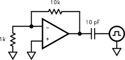
 Figure 30. Overload Recovery Test Circuit
The wide bandwidth of the LMP201x enhances performance when it is used as an amplifier to drive loads that inject transients back into the output. ADCs (Analog-to-Digital Converters) and multiplexers are examples of this type of load. To simulate this type of load, a pulse generator producing a 1-V peak square wave was connected to the output through a 10-pF capacitor. (Figure 30) The typical time for the output to recover to 1% of the applied pulse is 80 ns. To recover to 0.1% requires 860 ns. This rapid recovery is due to the wide bandwidth of the output stage and large total GBW.