ZHCSDC9D August   2012  – February 2015 LMH6882

PRODUCTION DATA.  

  1. 特性
  2. 应用
  3. 说明
  4. 修订历史记录
  5. Pin Configuration and Functions
  6. Specifications
    1. 6.1 Absolute Maximum Ratings
    2. 6.2 ESD Ratings
    3. 6.3 Recommended Operating Conditions
    4. 6.4 Thermal Information
    5. 6.5 Electrical Characteristics
    6. 6.6 Typical Characteristics
      1. 6.6.1 Single-Ended Input
  7. Detailed Description
    1. 7.1 Overview
    2. 7.2 Functional Block Diagram
    3. 7.3 Feature Description
    4. 7.4 Device Functional Modes
    5. 7.5 Programming
      1. 7.5.1 Digital Control of the Gain and Power-Down Pins
      2. 7.5.2 Parallel Interface
      3. 7.5.3 SPI-Compatible Serial Interface
  8. Application and Implementation
    1. 8.1 Application Information
      1. 8.1.1 Input Characteristics
      2. 8.1.2 Output Characteristics
      3. 8.1.3 Interfacing to an ADC
        1. 8.1.3.1 ADC Noise Filter
        2. 8.1.3.2 AC Coupling to an ADC
        3. 8.1.3.3 DC Coupling to an ADC
      4. 8.1.4 Figure of Merit: Dynamic Range Figure
    2. 8.2 Typical Applications
      1. 8.2.1 LMH6882 Typical Application
        1. 8.2.1.1 Design Requirements
        2. 8.2.1.2 Detailed Design Procedure
        3. 8.2.1.3 Application Curves
      2. 8.2.2 LMH6882 Used as Twisted Pair Cable Driver
        1. 8.2.2.1 Design Requirements
        2. 8.2.2.2 Detailed Design Procedure
        3. 8.2.2.3 Application Curves
  9. Power Supply Recommendations
  10. 10Layout
    1. 10.1 Layout Guidelines
      1. 10.1.1 Uncontrolled Impedance Traces
    2. 10.2 Layout Example
    3. 10.3 Thermal Considerations
  11. 11器件和文档支持
    1. 11.1 文档支持
      1. 11.1.1 相关文档 
    2. 11.2 商标
    3. 11.3 静电放电警告
    4. 11.4 术语表
  12. 12机械封装和可订购信息

封装选项

请参考 PDF 数据表获取器件具体的封装图。

机械数据 (封装 | 引脚)
  • NJK|36
散热焊盘机械数据 (封装 | 引脚)
订购信息

5 Pin Configuration and Functions

NJK Package
36-Pins WQFN
Top View
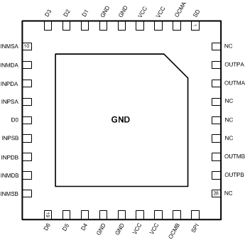
LMH6882 30202203.gif

Pin Functions

PIN TYPE DESCRIPTION
NAME NO.
ANALOG I/O
INPD, INMD 11, 12, 16, 17 Analog Input Differential inputs 100 Ω
INPS, INMS 10, 13, 15, 18 Analog Input Single ended inputs 50 Ω
OUTP, OUTM 35, 34, 30, 29 Analog Output Differential outputs, low impedance
POWER
GND 5, 6, 22, 23 Ground Ground pins. Connect to low-impedance ground plane. All pin voltages are specified with respect to the voltage on these pins. The exposed thermal pad is internally bonded to the ground pins.
VCC 3, 4, 24, 25 Power Power supply pins. Valid power supply range is 4.75 V to 5.25 V.
Exposed Center Pad Thermal/ Ground Thermal management/ Ground
DIGITAL INPUTS
SPI 27 Digital Input 0 = Parallel Mode, 1 = Serial Mode
PARALLEL MODE DIGITAL PINS, SPI = LOGIC LOW
D0, D1, D2, D3, D4, D5, D6 14, 7, 8, 9, 21, 29, 19 Digital Input Attenuator control, D0 = 0.25 dB, D6 = 16 dB
SD 1 Digital Input Shutdown 0 = amp on, 1 = amp off
SERIAL MODE DIGITAL PINS, SPI = LOGIC HIGH (SPI COMPATIBLE)
CS 9 Digital Input Chip Select (active low)
CLK 8 Digital Input Clock
SDO 14 Digital Output- Open Emitter Serial Data Output (Requires external bias.)
SDI 7 Digital Input Serial Data In