ZHCSGN3A September 2015 – October 2015 LM74670-Q1
PRODUCTION DATA.
8 Application and Implementation
NOTE
Information in the following applications sections is not part of the TI component specification, and TI does not warrant its accuracy or completeness. TI’s customers are responsible for determining suitability of components for their purposes. Customers should validate and test their design implementation to confirm system functionality.
8.1 Typical Rectifier Application
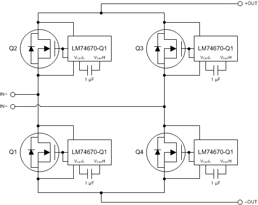
The LM74670-Q1 can be used with appropriate N-channel MOSFET to replace a diode in a typical rectifier application. The rectifier could be industrial for a 12/24AC supply or an automotive rectifier for a single phase or three phase field winding controlled alternator. The schematic for a typical implementation is shown in Figure 11 to implement a full bridge rectifier. The same schematic can also be extended to six legs for a three phase alternator rectification. Following considerations need to be made when selecting the appropriate MOSFET for this application:
1. An input voltage of 24V AC can reach a 34V peak. The MOSFET selected should have a VDS greater than this voltage.
2. The Continuous drain current of the MOSFET should be nearly 2.5X IAVG to cover peak currents during rectification.
3. The VGS(TH) threshold voltage of the selected MOSFET should be ≤3V to ensure error-free operation.
 Figure 11. Typical Full Bridge Rectifier Application
8.1.1 Design Requirements
For this design example, use the parameters listed in Table 1 as the input parameters
Table 1. Design Parameters
| DESIGN PARAMETER | EXAMPLE VALUE |
|---|---|
| Input Voltage Range | 4 – 42V peak AC |
| Output Voltage | rectified positive amplitude |
| Output current range | Maximum Drain current of MOSFET |
| Threshold voltage of FET VGS(TH) | 3V Max |
| Vcap value | 1µF |
8.1.2 Detailed Design Procedure
To begin the design process, determine the following:
8.1.2.1 Design Considerations
- Input voltage range
- Output current range
- Body Diode forward voltage drop for the selected MOSFET
- MOSFET Gate threshold voltage
8.1.2.2 Capacitor Selection
A ceramic capacitor should be placed between VcapL and VcapH. The capacitor acts as a holding tank to power up the control circuitry when the MOSFET is on.
When the MOSFET is off, this capacitor is charged up to higher voltage threshold of ~6.3V. Once this voltage is reached, the Gate Drive of LM74670-Q1 will provide drive for the external MOSFET. When the MOSFET is ON, the voltage across its body diode is collapsed because the forward conduction is through the MOSFET. During this time, the capacitor acts as a supply for the Gate Drive to keep the MOSFET ON.
The capacitor voltage will gradually decay when the MOSFET is ON. Once the capacitor voltage reaches a lower voltage threshold of 5.15V, the MOSFET is turned off and the capacitor gets recharged again for the next cycle.
A capacitor value of 220nF to 2.2uF with X7R/COG characteristic and 16V rating or higher is recommended for this application. A higher value capacitor sets longer MOSFET ON time and OFF time; however, the duty cycle remains at ~98% for MOSFET ON time irrespective of capacitor value.
If the Vcap value is 1µF, the MOSFET ON time and OFF time can be calculated using Equation 1 :
The duty cycle can be calculated using Equation 5 :
8.1.2.3 MOSFET Selection
The important MOSFET electrical parameters are the maximum continuous Drain current ID, the maximum drain-to-source voltage VDS(MAX), the gate-to-source threshold voltage VGS(TH) and the drain-to-source On resistance RDSON. The maximum continuous drain current, ID, rating must exceed the maximum continuous load current. The rating for the maximum current through the body diode, IS, is typically rated the same as, or slightly higher than the drain current, but body diode current only flows for a small period while the MOSFET gate is being charged to VGS(TH).The LM74670-Q1 can provide up to 5V VGS to drive the external MOSFET, therefore the VGS threshold of the selected MOSFET must be ≤ 3V.
The voltage across the MOSFET's body diode must be higher than 0.48V at low current. The body diode voltage for MOFETS typically decreases as the ambient temperature increases. This will increase the source current requirement to achieve the minimum body diode drain-to-source voltage for the charge pump to initiate. The maximum drain-to-source voltage, VDS(MAX), must be high enough to withstand the highest differential voltage seen in the application. This would include any anticipated fault conditions. Although there are no positive VDS limitation. However, it is recommended to use MOSFETS with voltage rating up to 45V for automotive applications, since the LM74670-Q1 has a reverse voltage limit of -45V. Table 2 shows the examples of recommended MOSFETs to be used with the LM74670-Q1.
8.1.3 Application Curves
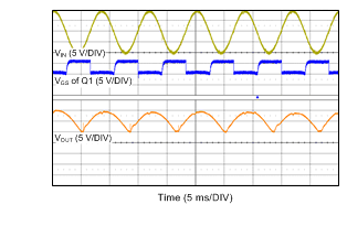
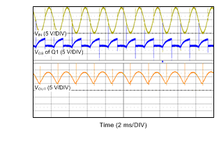
In the following plots, the input voltage is 20V AC. The output current is 5A for all frequencies.
 Figure 12. Response to 60Hz AC Input
 Figure 13. Response to 100Hz AC Input
 Figure 14. Response to a 300Hz AC Input
8.2 Design Requirements
NOTE
Startup voltage is the voltage drop is needed for the controller to turn ON. It directly influences the Minimum output current at which the MOSFET turns ON.
Table 2. Recommended MOSFET Examples(1)
| Part No | Voltage (V) Current |
Drain Current at 25C |
Rdson mΩ @ 4.5V |
Vgs Threshold (V) |
Diode Voltage @ 2A at 125C/175C |
Package; Footprint | Qual | |
|---|---|---|---|---|---|---|---|---|
| CSD17313Q2Q1 | 30 | 5 | 26 | 1.8 | 0.65 | SON; 2 x 2 | Auto | |
| SQJ886EP | 40 | 60 | 5.5 | 2.5 | 0.5 | PowerPAK SO-8L; 5 x 6 | Auto | |
| SQ4184EY | 40 | 29 | 5.6 | 2.5 | 0.5 | SO-8; 5 x 6 | Auto | |
| Si4122DY | 40 | 23.5 | 6 | 2.5 | 0.5 | SO-8; 5 x 6 | Auto | |
| RS1G120MN | 40 | 12 | 20.7 | 2.5 | 0.6 | HSOP8; 5 x 6 | Auto | |
| RS1G300GN | 40 | 30 | 2.5 | 2.5 | 0.5 | HSOP8; 5 x 6 | Auto | |
| CSD18501Q5A | 40 | 22 | 3.3 | 2.3 | 0.53 | SON; 5 x 6 | Industrial | |
| SQD40N06-14L | 60 | 40 | 17 | 2.5 | 0.5 | TO-252; 6 x 10 | Auto | |
| SQ4850EY | 60 | 12 | 31 | 2.5 | 0.55 | SO-8; 5 x 6 | Auto | |
| CSD18532Q5B | 60 | 23 | 3.3 | 2.2 | 0.53 | SON;5 x 6 | Industrial | |
| IPG20N04S4L-07A | 40 | 20 | 7.2 | 2.2 | 0.48 | PG-TDSON-8-10; 5 x 6 | Auto | |
| IPB057N06N | 60 | 45 | 5.7 | 3.3 | 0.55 | PG-TO263-3; 10 x 15 | Auto | |
| IPD50N04S4L | 40 | 50 | 7.3 | 2.2 | 0.50 | PG-TO252-3-313; 6 x10 | Auto | |
| BUK9Y3R5-40E | 40 | 100 | 3.8 | 2.1 | 0.48 | LFPAK56; Power-SO8 (SOT669); 5 x 6 | Auto | |
| IRF7478PbF-1 | 60 | 7 | 30 | 3 | 0.55 | SO-8; 5 x 6 | Industrial | |
| SQJ422EP | 40 | 75 | 4.3 | 2.5 | 0.50 | PowerPAK SO-8L; 5 x 6 | Auto | |
| IRL1004 | 40 | 130 | 6.5 | 1 | 0.60 | TO-220AB | Auto | |
| AUIRL7736 | 40 | 112 | 2.2 | 3 | 0.65 | DirectFET®; 5 x 6 | Auto | |