SNOS752E May 1999 – September 2014 LM6152 , LM6154
PRODUCTION DATA.
- 1Features
- 2Applications
- 3Description
- 4Revision History
- 5Pin Configuration and Functions
-
6Specifications
- 6.1 Absolute Maximum Ratings
- 6.2 Handling Ratings
- 6.3 Recommended Operating Conditions
- 6.4 Thermal Information
- 6.5 5.0 V DC Electrical Characteristics
- 6.6 5.0 V AC Electrical Characteristics
- 6.7 2.7 V DC Electrical Characteristics
- 6.8 2.7 V AC Electrical Characteristics
- 6.9 24 V DC Electrical Characteristics
- 6.10 24 V AC Electrical Characteristics
- 6.11 Typical Performance Characteristics
- 7Application and Implementation
- 8Device and Documentation Support
- 9Mechanical, Packaging, and Orderable Information
7 Application and Implementation
The LM6152/LM6154 is ideally suited for operation with about 10 kΩ (Feedback Resistor, RF) between the output and the negative input terminal.
With RF set to this value, for most applications requiring a close loop gain of 10 or less, an additional small compensation capacitor (CF) (see Figure 26) is recommended across RF in order to achieve a reasonable overshoot (10%) at the output by compensating for stray capacitance across the inputs.
The optimum value for CF can best be established experimentally with a trimmer cap in place since its value is dependant on the supply voltage, output driving load, and the operating gain. Below, some typical values used in an inverting configuration and driving a 10 kΩ load have been tabulated for reference:
Table 1. Typical BW (−3 dB) at Various
Supply Voltage and Gains
| VS
Volts |
GAIN | CF
pF |
BW (−3 dB) MHz |
|---|---|---|---|
| 3 | −1 | 5.6 | 4 |
| −10 | 6.8 | 1.97 | |
| −100 | None | 0.797 | |
| 24 | −1 | 2.2 | 6.6 |
| −10 | 4.7 | 2.2 | |
| −100 | None | 0.962 |
In the non-inverting configuration, the LM6152/LM6154 can be used for closed loop gains of +2 and above. In this case, also, the compensation capacitor (CF) is recommended across RF (= 10 kΩ) for gains of 10 or less.
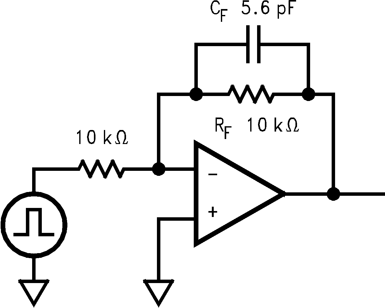 Figure 26. Typical Inverting Gain Circuit AV = −1
Because of the unique structure of this amplifier, when used at low closed loop gains, the realizable BW will be much less than the GBW product would suggest.
The LM6152/LM6154 brings a new level of ease of use to op amp system design.
The greater than rail-to-rail input voltage range eliminates concern over exceeding the common-mode voltage range. The rail-to-rail output swing provides the maximum possible dynamic range at the output. This is particularly important when operating on low supply voltages.
The high gain-bandwidth with low supply current opens new battery powered applications where higher power consumption previously reduced battery life to unacceptable levels.
The ability to drive large capacitive loads without oscillating functional removes this common problem.
To take advantage of these features, some ideas should be kept in mind.
The LM6152/LM6154, capacitive loads do not lead to oscillations, in all but the most extreme conditions, but they will result in reduced bandwidth. They also cause increased settling time.
Unlike most bipolar op amps, the unique phase reversal prevention/speed-up circuit in the input stage, causes the slew rate to be very much a function of the input pulse amplitude. This results in a 10 to 1 increase in slew rate when the differential input signal increases. Large fast pulses will raise the slew-rate to more than 30 V/µs.
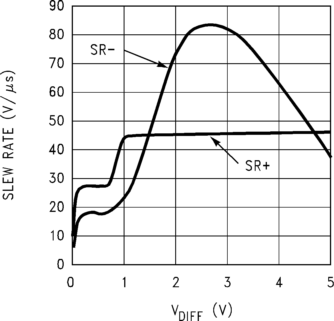 Figure 27. Slew Rate vs. VDIFF
The speed-up action adds stability to the system when driving large capacitive loads.
A conventional op amp exhibits a fixed maximum slew-rate even though the differential input voltage rises due to the lagging output voltage. In the LM6152/LM6154, increasing lag causes the differential input voltage to increase but as it does, the increased slew-rate keeps the output following the input much better. This effectively reduces phase lag. As a result, the LM6152/LM6154 can drive capacitive loads as large as 470 pF at gain of 2 and above, and not oscillate.
Capacitive loads decrease the phase margin of all op amps. This can lead to overshoot, ringing and oscillation. This is caused by the output resistance of the amplifier and the load capacitance forming an R-C phase shift network. The LM6152/6154 senses this phase shift and partly compensates for this effect.