SNAS548D February 2000 – January 2015 LM555
PRODUCTION DATA.
- 1 Features
- 2 Applications
- 3 Description
- 4 Revision History
- 5 Pin Configuration and Functions
- 6 Specifications
- 7 Detailed Description
- 8 Application and Implementation
- 9 Power Supply Recommendations
- 10Layout
- 11Device and Documentation Support
- 12Mechanical, Packaging, and Orderable Information
封装选项
机械数据 (封装 | 引脚)
散热焊盘机械数据 (封装 | 引脚)
订购信息
6 Specifications
6.1 Absolute Maximum Ratings
over operating free-air temperature range (unless otherwise noted)(1)(2)| MIN | MAX | UNIT | |||
|---|---|---|---|---|---|
| Power Dissipation(3) | LM555CM, LM555CN(4) | 1180 | mW | ||
| LM555CMM | 613 | mW | |||
| Soldering Information | PDIP Package | Soldering (10 Seconds) | 260 | °C | |
| Small Outline Packages (SOIC and VSSOP) | Vapor Phase (60 Seconds) | 215 | °C | ||
| Infrared (15 Seconds) | 220 | °C | |||
| Storage temperature, Tstg | –65 | 150 | °C | ||
(1) Stresses beyond those listed under Absolute Maximum Ratings may cause permanent damage to the device. These are stress ratings only, which do not imply functional operation of the device at these or any other conditions beyond those indicated under Recommended Operating Conditions. Exposure to absolute-maximum-rated conditions for extended periods may affect device reliability.
(2) If Military/Aerospace specified devices are required, please contact the TI Sales Office/Distributors for availability and specifications.
(3) For operating at elevated temperatures the device must be derated above 25°C based on a 150°C maximum junction temperature and a thermal resistance of 106°C/W (PDIP), 170°C/W (S0IC-8), and 204°C/W (VSSOP) junction to ambient.
(4) Refer to RETS555X drawing of military LM555H and LM555J versions for specifications.
6.2 ESD Ratings
| VALUE | UNIT | |||
|---|---|---|---|---|
| V(ESD) | Electrostatic discharge | Human-body model (HBM), per ANSI/ESDA/JEDEC JS-001(1) | ±500(2) | V |
(1) JEDEC document JEP155 states that 500-V HBM allows safe manufacturing with a standard ESD control process.
(2) The ESD information listed is for the SOIC package.
6.3 Recommended Operating Conditions
over operating free-air temperature range (unless otherwise noted)| MIN | MAX | UNIT | ||
|---|---|---|---|---|
| Supply Voltage | 18 | V | ||
| Temperature, TA | 0 | 70 | °C | |
| Operating junction temperature, TJ | 70 | °C | ||
6.4 Thermal Information
| THERMAL METRIC(1) | LM555 | UNIT | |||
|---|---|---|---|---|---|
| PDIP | SOIC | VSSOP | |||
| 8 PINS | |||||
| RθJA | Junction-to-ambient thermal resistance | 106 | 170 | 204 | °C/W |
(1) For more information about traditional and new thermal metrics, see the IC Package Thermal Metrics application report, SPRA953.
6.5 Electrical Characteristics
(TA = 25°C, VCC = 5 V to 15 V, unless otherwise specified)(1)(2)| PARAMETER | TEST CONDITIONS | MIN | TYP | MAX | UNIT |
|---|---|---|---|---|---|
| Supply Voltage | 4.5 | 16 | V | ||
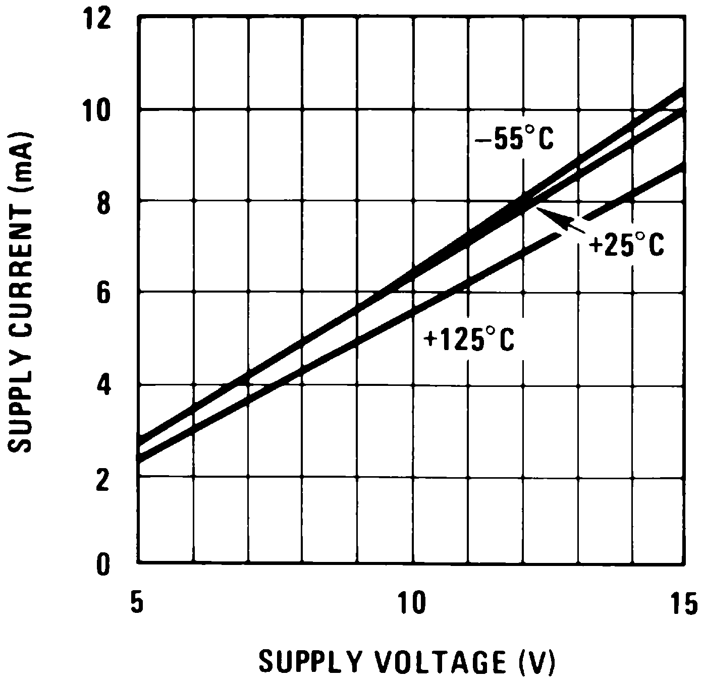
| Supply Current | VCC = 5 V, RL = ∞ | 3 | 6 | mA | |
| VCC = 15 V, RL = ∞ (Low State) (3) |
10 | 15 | |||
| Timing Error, Monostable | |||||
| Initial Accuracy | 1 % | ||||
| Drift with Temperature | RA = 1 k to 100 kΩ, | 50 | ppm/°C | ||
| C = 0.1 μF, (4) | |||||
| Accuracy over Temperature | 1.5 % | ||||
| Drift with Supply | 0.1 % | V | |||
| Timing Error, Astable | |||||
| Initial Accuracy | 2.25 | ||||
| Drift with Temperature | RA, RB =1 k to 100 kΩ, | 150 | ppm/°C | ||
| C = 0.1 μF, (4) | |||||
| Accuracy over Temperature | 3.0% | ||||
| Drift with Supply | 0.30 % | /V | |||
| Threshold Voltage | 0.667 | x VCC | |||
| Trigger Voltage | VCC = 15 V | 5 | V | ||
| VCC = 5 V | 1.67 | V | |||
| Trigger Current | 0.5 | 0.9 | μA | ||
| Reset Voltage | 0.4 | 0.5 | 1 | V | |
| Reset Current | 0.1 | 0.4 | mA | ||
| Threshold Current | (5) | 0.1 | 0.25 | μA | |
| Control Voltage Level | VCC = 15 V | 9 | 10 | 11 | V |
| VCC = 5 V | 2.6 | 3.33 | 4 | ||
| Pin 7 Leakage Output High | 1 | 100 | nA | ||
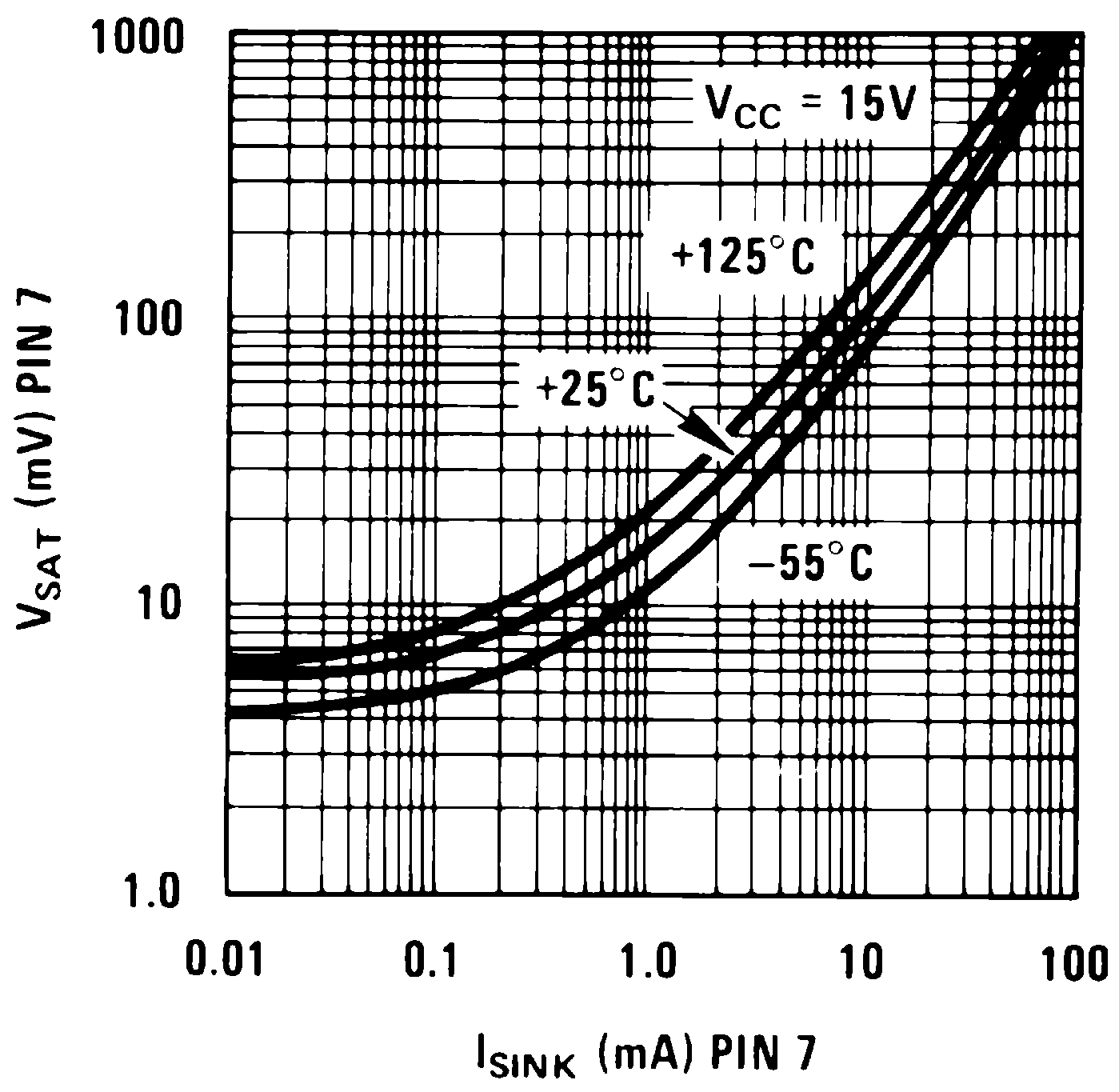
| Pin 7 Sat (6) | |||||
| Output Low | VCC = 15 V, I7 = 15 mA | 180 | mV | ||
| Output Low | VCC = 4.5 V, I7 = 4.5 mA | 80 | 200 | mV | |
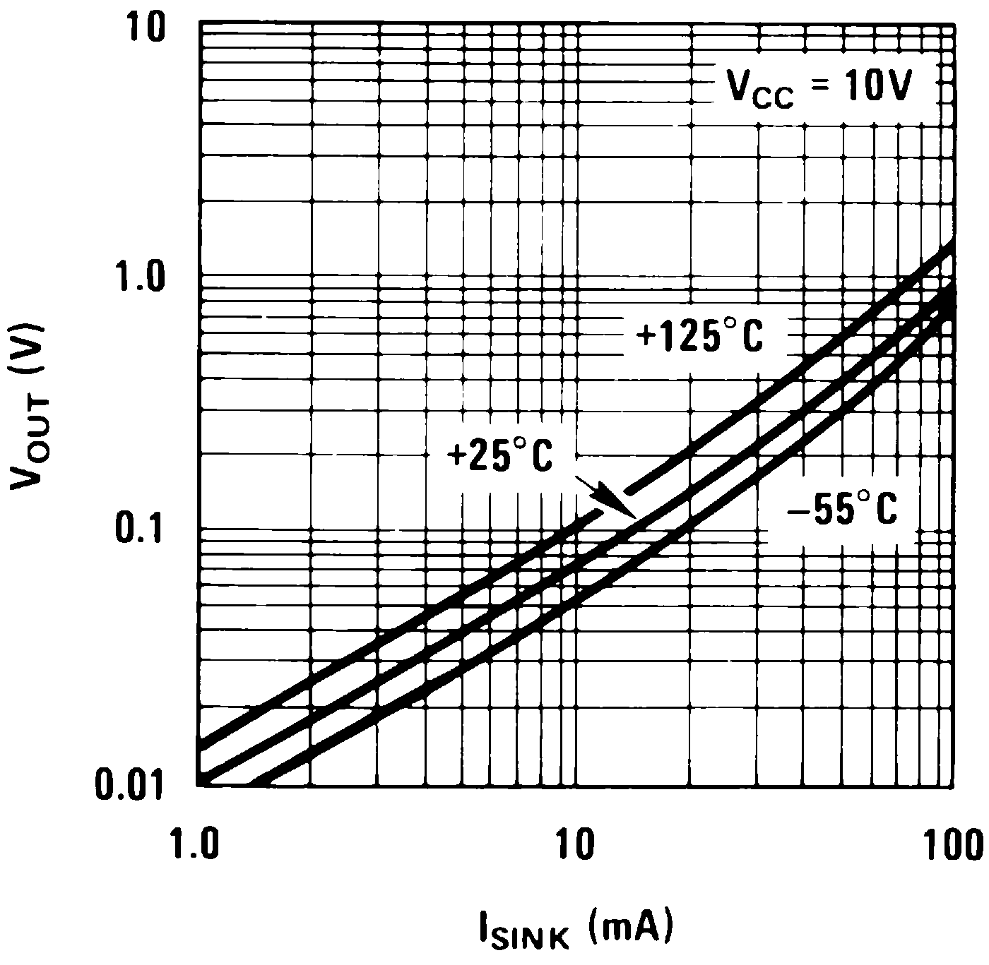
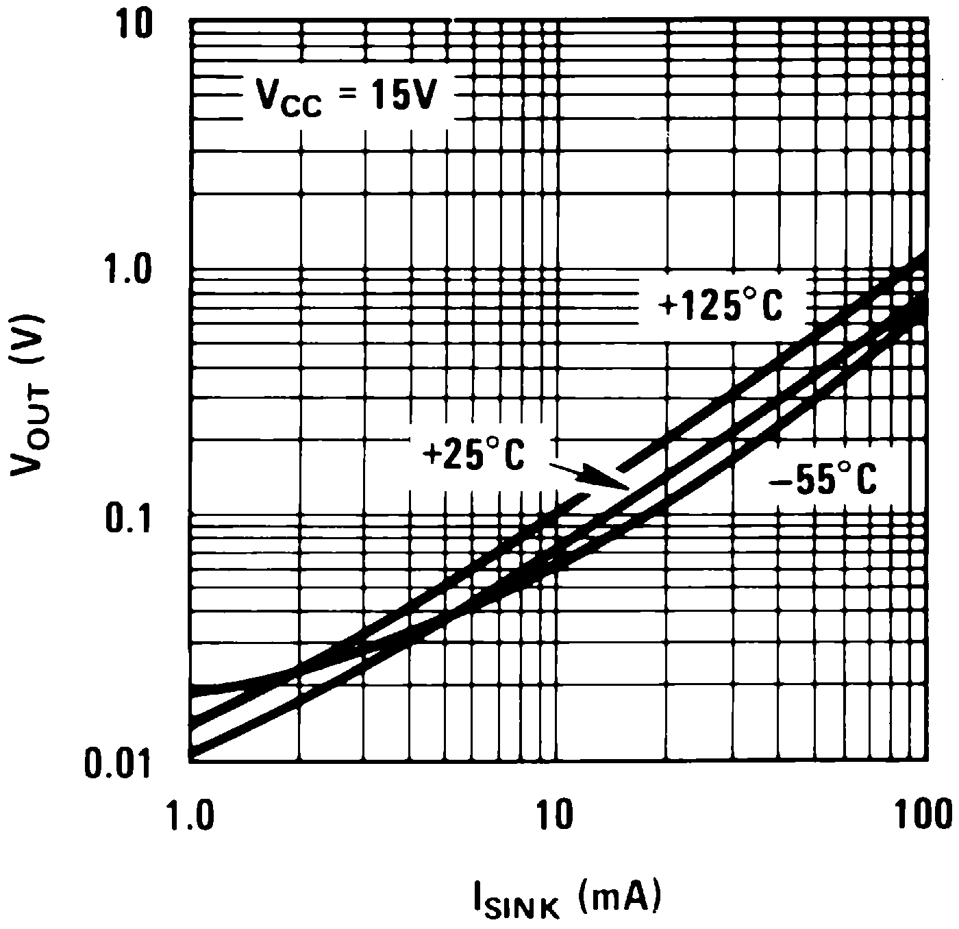
| Output Voltage Drop (Low) | VCC = 15 V | ||||
| ISINK = 10 mA | 0.1 | 0.25 | V | ||
| ISINK = 50 mA | 0.4 | 0.75 | V | ||
| ISINK = 100 mA | 2 | 2.5 | V | ||
| ISINK = 200 mA | 2.5 | V | |||
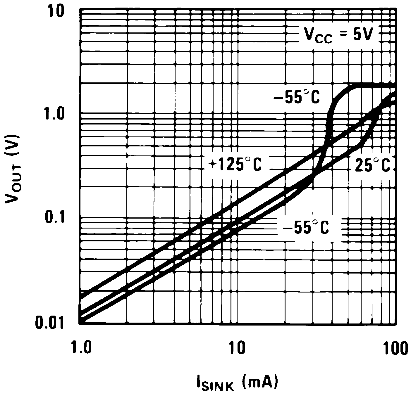
| VCC = 5 V | |||||
| ISINK = 8 mA | V | ||||
| ISINK = 5 mA | 0.25 | 0.35 | V | ||
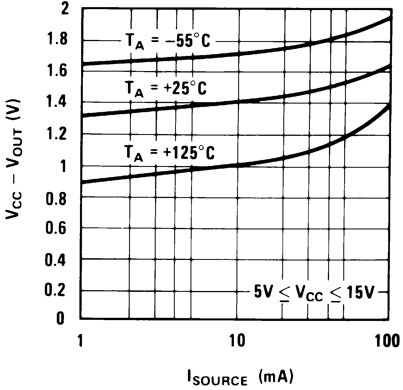
| Output Voltage Drop (High) | ISOURCE = 200 mA, VCC = 15 V | 12.5 | V | ||
| ISOURCE = 100 mA, VCC = 15 V | 12.75 | 13.3 | V | ||
| VCC = 5 V | 2.75 | 3.3 | V | ||
| Rise Time of Output | 100 | ns | |||
| Fall Time of Output | 100 | ns |
(1) All voltages are measured with respect to the ground pin, unless otherwise specified.
(2) Absolute Maximum Ratings indicate limits beyond which damage to the device may occur. Recommended Operating Conditions indicate conditions for which the device is functional, but do not ensure specific performance limits. Electrical Characteristics state DC and AC electrical specifications under particular test conditions which ensures specific performance limits. This assumes that the device is within the Recommended Operating Conditions. Specifications are not ensured for parameters where no limit is given, however, the typical value is a good indication of device performance.
(3) Supply current when output high typically 1 mA less at VCC = 5 V.
(4) Tested at VCC = 5 V and VCC = 15 V.
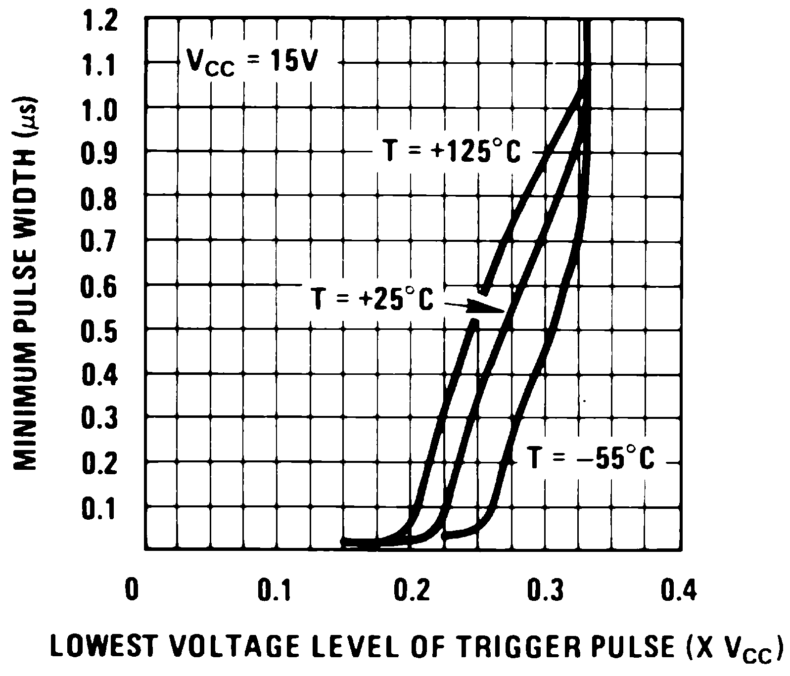
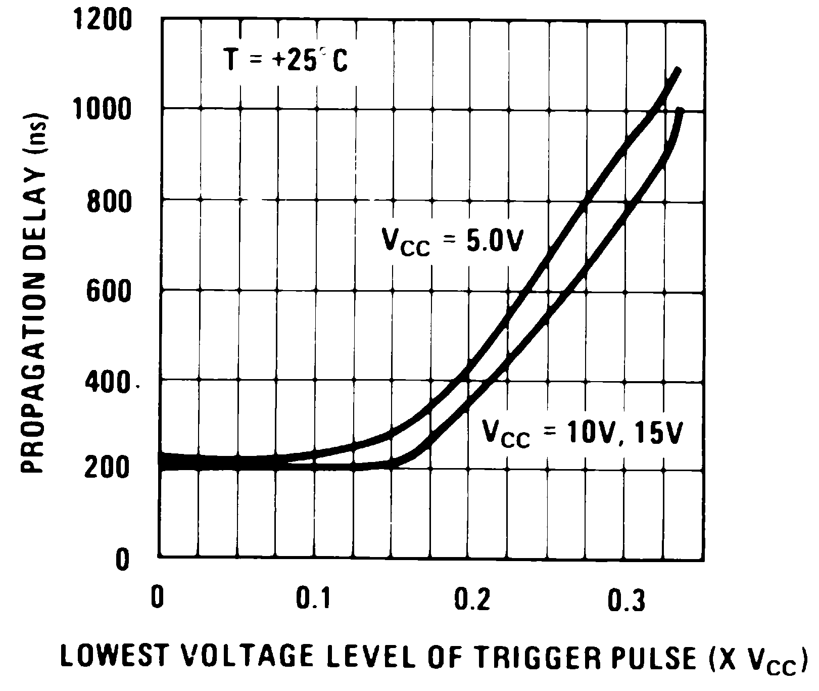
(5) This will determine the maximum value of RA + RB for 15 V operation. The maximum total (RA + RB) is 20 MΩ.
(6) No protection against excessive pin 7 current is necessary providing the package dissipation rating will not be exceeded.
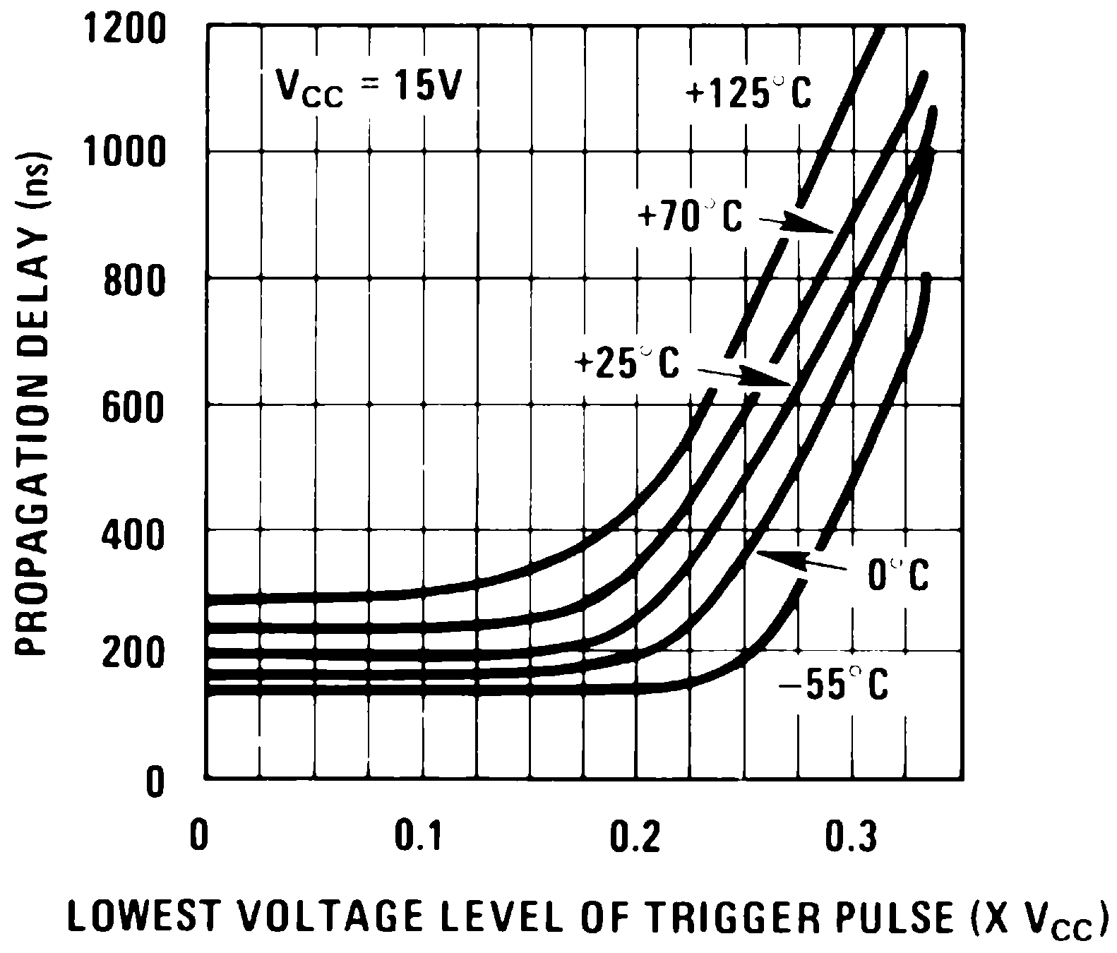
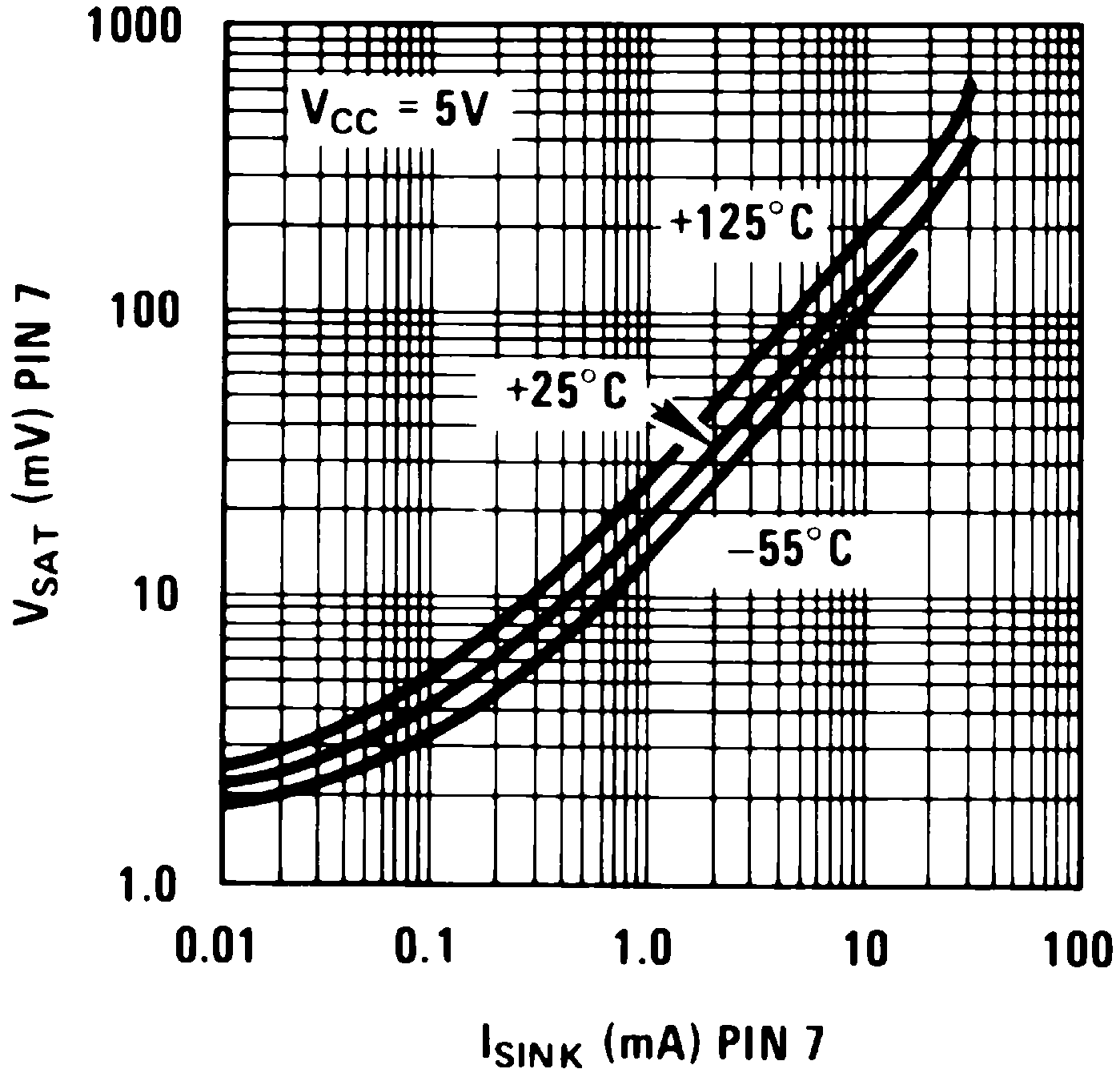
6.6 Typical Characteristics