SNAS548D February 2000 – January 2015 LM555
PRODUCTION DATA.
- 1 Features
- 2 Applications
- 3 Description
- 4 Revision History
- 5 Pin Configuration and Functions
- 6 Specifications
- 7 Detailed Description
- 8 Application and Implementation
- 9 Power Supply Recommendations
- 10Layout
- 11Device and Documentation Support
- 12Mechanical, Packaging, and Orderable Information
封装选项
机械数据 (封装 | 引脚)
散热焊盘机械数据 (封装 | 引脚)
订购信息
10 Layout
10.1 Layout Guidelines
Standard PCB rules apply to routing the LM555. The 0.1-µF capacitor in parallel with a 1-µF electrolytic capacitor should be as close as possible to the LM555. The capacitor used for the time delay should also be placed as close to the discharge pin. A ground plane on the bottom layer can be used to provide better noise immunity and signal integrity.
Figure 20 is the basic layout for various applications.
- C1 – based on time delay calculations
- C2 – 0.01-µF bypass capacitor for control voltage pin
- C3 – 0.1-µF bypass ceramic capacitor
- C4 – 1-µF electrolytic bypass capacitor
- R1 – based on time delay calculations
- U1 – LMC555
10.2 Layout Example
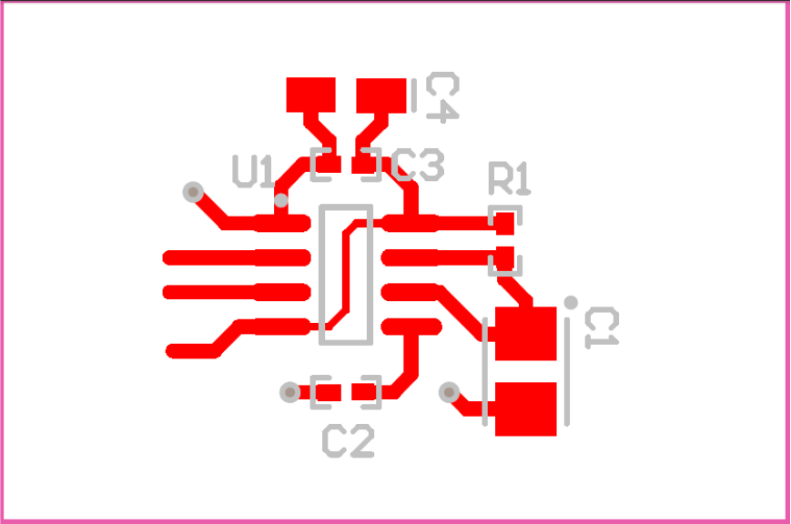 Figure 20. Layout Example