ZHCSL47A April 2020 – January 2021 LM5181
PRODUCTION DATA
- 1 特性
- 2 应用
- 3 说明
- 4 Revision History
- 5 Description (continued)
- 6 Pin Configuration and Functions
- 7 Specifications
-
8 Detailed Description
- 8.1 Overview
- 8.2 Functional Block Diagram
- 8.3
Feature Description
- 8.3.1 Integrated Power MOSFET
- 8.3.2 PSR Flyback Modes of Operation
- 8.3.3 Setting the Output Voltage
- 8.3.4 Control Loop Error Amplifier
- 8.3.5 Precision Enable
- 8.3.6 Configurable Soft Start
- 8.3.7 External Bias Supply
- 8.3.8 Minimum On-Time and Off-Time
- 8.3.9 Overcurrent Protection
- 8.3.10 Thermal Shutdown
- 8.4 Device Functional Modes
-
9 Application and Implementation
- 9.1 Application Information
- 9.2
Typical Applications
- 9.2.1
Design 1: Wide VIN, Low IQ PSR Flyback Converter Rated at 5 V, 0.5 A
- 9.2.1.1 Design Requirements
- 9.2.1.2
Detailed Design Procedure
- 9.2.1.2.1 Custom Design With WEBENCH® Tools
- 9.2.1.2.2 Custom Design With Excel Quickstart Tool
- 9.2.1.2.3 Flyback Transformer – T1
- 9.2.1.2.4 Flyback Diode – DFLY
- 9.2.1.2.5 Zener Clamp Circuit – DF, DCLAMP
- 9.2.1.2.6 Output Capacitor – COUT
- 9.2.1.2.7 Input Capacitor – CIN
- 9.2.1.2.8 Feedback Resistor – RFB
- 9.2.1.2.9 Thermal Compensation Resistor – RTC
- 9.2.1.2.10 UVLO Resistors – RUV1, RUV2
- 9.2.1.2.11 Soft-Start Capacitor – CSS
- 9.2.2 Application Curves
- 9.2.1
Design 1: Wide VIN, Low IQ PSR Flyback Converter Rated at 5 V, 0.5 A
- 10Power Supply Recommendations
- 11Layout
- 12Device and Documentation Support
- 13Mechanical, Packaging, and Orderable Information
9.2.1.2.7 Input Capacitor – CIN
Select an input capacitance using Equation 24 to limit the ripple voltage amplitude to less than 5% of the input voltage when operating at nominal input voltage.
Equation 24. 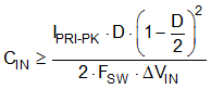
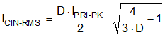
Substituting the input current at full load, switching frequency, peak primary current, and peak-to-peak ripple specification gives CIN greater than 1 μF. Mindful of the voltage coefficient of ceramic capacitors, select a 2.2-µF, 100-V ceramic input capacitor with X7R dielectric in 1210 case size. Equation 25 gives the input capacitor RMS ripple current.
Equation 25.