ZHCSHU0C March 2018 – October 2021 LM51501-Q1
PRODUCTION DATA
- 1 特性
- 2 应用
- 3 说明
- 4 Revision History
- 5 Device Comparison Table
- 6 Pin Configuration and Functions
- 7 Specifications
-
8 Detailed Description
- 8.1 Overview
- 8.2 Functional Block Diagram
- 8.3
Feature Description
- 8.3.1 Enable (EN Pin)
- 8.3.2 High Voltage VCC Regulator (PVCC, AVCC Pin)
- 8.3.3 Power-On Voltage Selection (VSET Pin)
- 8.3.4 Switching Frequency (RT Pin)
- 8.3.5 Clock Synchronization (SYNC Pin in SS Configuration)
- 8.3.6 Current Sense, Slope Compensation, and PWM (CS Pin)
- 8.3.7 Current Limit (CS Pin)
- 8.3.8 Feedback and Error Amplifier (COMP Pin)
- 8.3.9 Automatic Wake-Up and Standby
- 8.3.10 Boost Status Indicator (STATUS Pin)
- 8.3.11 Maximum Duty Cycle Limit and Minimum Input Supply Voltage
- 8.3.12 MOSFET Driver (LO Pin)
- 8.3.13 Thermal Shutdown
- 8.4 Device Functional Modes
-
9 Application and Implementation
- 9.1 Application Information
- 9.2
Typical Application
- 9.2.1 Design Requirements
- 9.2.2
Detailed Design Procedure
- 9.2.2.1 Custom Design With WEBENCH® Tools
- 9.2.2.2 RSET Resistor
- 9.2.2.3 RT Resistor
- 9.2.2.4 Inductor Selection (LM)
- 9.2.2.5 Current Sense (RS)
- 9.2.2.6 Slope Compensation Ramp (RSL)
- 9.2.2.7 Output Capacitor (COUT)
- 9.2.2.8 Loop Compensation Component Selection and Maximum ESR
- 9.2.2.9 PVCC Capacitor, AVCC Capacitor, and AVCC Resistor
- 9.2.2.10 VOUT Filter (CVOUT, RVOUT)
- 9.2.2.11 Input Capacitor
- 9.2.2.12 MOSFET Selection
- 9.2.2.13 Diode Selection
- 9.2.2.14 Efficiency Estimation
- 9.2.3 Application Curves
- 9.3 System Examples
- 10Power Supply Recommendations
- 11Layout
- 12Device and Documentation Support
- 13Mechanical, Packaging, and Orderable Information
9.2.2.4 Inductor Selection (LM)
When selecting the inductor, consider three key parameters: inductor current ripple ratio (RR), falling slope of the inductor current, and RHP zero frequency (FRHP).
Inductor current ripple ratio is selected to have a balance between core loss and copper loss. The falling slope of the inductor current must be low enough to prevent subharmonic oscillation at high duty cycle (additional RSL resistor is required, if not). Higher FRHP (= lower inductance) allows a higher crossover frequency and is always preferred when using a smaller value output capacitor.
The inductance value can be selected to set the inductor current ripple between 30% and 70% of the average inductor current as a good compromise between RR, FRHP, and inductor falling slope. In this example, 60% ripple ratio (RR = 0.6) is selected as the maximum inductor current ripple ratio (the inductor current ripple ratio is the biggest when D = 0.33). The target inductance value is calculated using Equation 20:
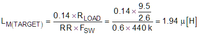
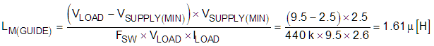
If the target inductance is smaller than the value calculated using Equation 20, consider adding the slope compensation resistor (RSL), as mentioned in Section 9.2.2.6, or select a smaller RR and recalculate the inductance using Equation 21.
A standard value of 2.2 µH is chosen for LM. The required inductor saturation current rating is estimated after selecting RS and RSL.