SNVS363E August 2005 – November 2015 LM5026
PRODUCTION DATA.
- 1 Features
- 2 Applications
- 3 Description
- 4 Revision History
- 5 Pin Configuration and Functions
- 6 Specifications
-
7 Detailed Description
- 7.1 Overview
- 7.2 Functional Block Diagram
- 7.3
Feature Description
- 7.3.1 High Voltage Start-Up Regulator
- 7.3.2 Line Undervoltage Detector
- 7.3.3 PWM Outputs
- 7.3.4 Gate Driver Outputs
- 7.3.5 PWM Comparator/Slope Compensation
- 7.3.6 Maximum Duty Cycle Clamp
- 7.3.7 Soft-Start / Soft-Stop
- 7.3.8 Current Sense and Current Limit
- 7.3.9 Overload Protection Timer
- 7.3.10 Oscillator and Sync Capability
- 7.3.11 Thermal Protection
- 7.4 Device Functional Modes
-
8 Application and Implementation
- 8.1 Application Information
- 8.2 Typical Application
- 9 Power Supply Recommendations
- 10Layout
- 11Device and Documentation Support
- 12Mechanical, Packaging, and Orderable Information
8 Application and Implementation
NOTE
Information in the following applications sections is not part of the TI component specification, and TI does not warrant its accuracy or completeness. TI’s customers are responsible for determining suitability of components for their purposes. Customers should validate and test their design implementation to confirm system functionality.
8.1 Application Information
8.1.1 Line Input (VIN)
The LM5026 contains an internal high voltage start-up regulator that allows the input pin (VIN) to be connected directly to a nominal 48-V line voltage. The voltage applied to the VIN pin can vary in the range of 13 to 100 V with transient capability to 105 V. When power is applied and the UVLO pin potential is greater than 0.4 V, the VCC regulator is enabled and sources current into an external capacitor connected to the VCC pin. When the voltage on the VCC pin reaches the regulation point of 7.7 V, the internal voltage reference (REF) is enabled. The reference regulation set-point is 5 V. The controller outputs are enabled when the UVLO pin potential is greater than 1.25 V. In typical applications, an auxiliary transformer winding is connected through a diode to the VCC pin. This winding must raise the VCC voltage above 8 V to shut off the internal start-up regulator. TI recommends a filtering circuit shown in Figure 24 be used to suppress transients, which may occur at the input supply, in particular when VIN is operated close to the maximum operating rating.
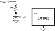 Figure 24. Input Transient Protection
8.1.2 For Application > 100 V
For applications where the system input voltage exceed 100 V or IC power dissipation is a concern, the LM5026 can be powered from an external start-up regulator as shown in Figure 25. In this configuration, the VIN and the VCC pins should be connected together, which allows the LM5026 to be operated below 13 V. The voltage at the VCC pin must be greater than 8 V yet not exceed 15 V. An auxiliary winding can be used to reduce the dissipation in the external regulator once the power converter is active.
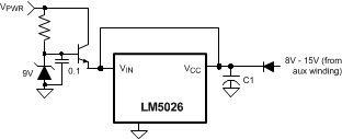 Figure 25. Start-Up Regulator for VPWR >100 V
8.1.3 Undervoltage Lockout (UVLO)
When the UVLO pin voltage is below 0.4 V, the controller is in a low current shutdown mode. When the UVLO pin voltage is greater than 0.4 V but less than 1.25 V, the controller is in standby mode. When the UVLO pin voltage is greater than 1.25 V, the controller is fully enabled. Typically, two external resistors program the minimum operational voltage for the power converter as shown in Figure 26. When UVLO pin voltage is above the 1.25-V threshold, an internal 20-μA current source is enabled to raise the voltage at the UVLO pin, thus providing threshold hysteresis. Resistance values for R1 and R2 can be determined from Equation 6 and Equation 7:

where
- VHYS is the desired UVLO hysteresis at VPWR
.

where
- VPWR is the desired turnon voltage
For example, if the LM5026 is to be enabled when VPWR reaches 33 V, and disabled when VPWR is decreased to 30 V, R1 calculates to 150 kΩ, and R2 calculates to 5.9 kΩ. The voltage at the UVLO pin should not exceed 6 V at any time. Be sure to check both the power and voltage rating for the selected R1 resistor.
Remote configuration of the controller’s operational modes can be accomplished with open drain device(s) connected to the UVLO pin as shown in Figure 27.
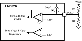 Figure 26. Basic UVLO Configuration
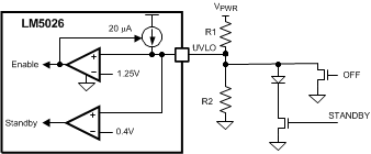 Figure 27. Remote Standby and Disable Control
8.1.4 Oscillator (RT, SYNC)
Oscillator (RT, SYNC) The oscillator frequency is generally selected in conjunction with the design of the system magnetic components along with the volume and efficiency goals for a given power converter design. The total RT resistance at the RT pin sets the oscillator frequency. The RT resistors should be one of the first components placed and connected when designing the PCB. Direct, short connections to each side of the RT resistors (RT, DCL and AGND pins) are recommended .
The SYNC pin can be used to synchronize the internal oscillator to an external clock. An open-drain output is the recommended interface from the external clock to the SYNC pin. The clock pulse width should be greater than 15 ns. The external clock must be a higher frequency than the free-running frequency set by the RT resistor. Multiple LM5026 devices can be synchronized together simply by connecting the devices SYNC pins together. Take care to ensure the ground potential differences between devices are minimized. In this configuration all of the devices will be synchronized to the highest frequency device.
8.1.5 Voltage Feedback (COMP)
The COMP pin is designed to accept the voltage loop feedback error signal from the regulated output through an error amplifier and (typically) an optocoupler. In a typical configuration, VOUT is compared to a precision reference voltage by the error amplifier. The output of the amplifier drives the optocoupler, which in turn drives the COMP pin. The parasitic capacitance of the optocoupler often limits the achievable loop bandwidth for a given power converter. The optocoupler LED and detector junction capacitance produce a low-frequency pole in the voltage regulation loop. The LM5026 current controlled optocoupler interface (COMP) previously described, greatly increases the pole frequency associated with the optocoupler.
8.1.6 Current Sense (CS)
The CS pin receives an input signal representative of the transformer primary current, either from a current sense transformer (Figure 28) or from a resistor in series with the source of the primary switch (Figure 29). In both cases the sensed current creates a ramping voltage across R1, while the RF/CF filter suppresses noise and transients. R1, RF and CF should be as physically close to the LM5026 as possible, and the ground connection from the current sense transformer, or R1, should be a dedicated track to the AGND pin. The current-sense components must provide > 0.5 V at the CS pin when an overcurrent condition exists.
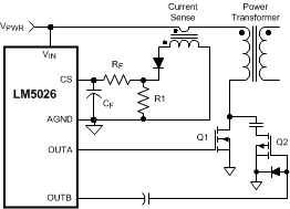 Figure 28. Current Sense Using a Current-Sense Transformer
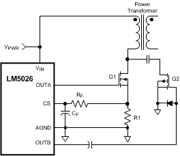 Figure 29. Current Sense Using a Source-Sense Resistor (R1)
8.1.7 Hiccup Mode Current Limit Restart (RES)
The basic operation of the hiccup mode current limit restart is described in the functional description. The delay time to restart is programmed with the selection of the RES pin capacitor CRES as shown in Figure 19. In the case of continuous cycle-by-cycle current limit detection at the CS pin, the time required for CRES to reach the 2.5-V hiccup mode threshold is calculated by Equation 8 :

For example, if CRES = 0.01 µF, the time t1 is approximately 2.5 ms.
The cool down time, t2 is set by the soft-start capacitor (CSS) and the internal 1-µA SS current source, and is equal to Equation 9:

If CSS = 0.01 µF, t2 is approximately 14 ms.
The soft-start time t3 is set by the internal 50-µA current source, and is equal to Equation 10:

The time t2 provides a periodic cool-down time for the power converter in the event of a sustained overload or short circuit. This results in lower average input current and lower power dissipated within the power components. It is recommended that the ratio of t2/(t1 + t3) be in the range of 5 to 10 to make good use of this feature. If the application requires no delay from the first detection of a current limit condition to the onset of the hiccup mode (t1 = 0), the RES pin can be left open (no external capacitor). If it is desired to disable the hiccup mode current limit operation, the RES pin should be connected to ground (AGND).
8.1.8 Soft-Start (SS)
An internal current source and an external soft-start capacitor determines the time required for the output duty cycle to increase from zero to its final value for regulation. The minimum acceptable time is dependent on the output capacitance and the response of the feedback loop. If the soft-start time is too quick, the output could overshoot its intended voltage before the feedback loop can regulate the PWM controller. After power is applied and the controller is fully enabled, the voltage at the SS pin ramps up as CSS is charged by an internal 50-µA current source. The voltage at the output of the COMP pin current mirror is clamped to the same potential as the SS pin by a voltage buffer with a sink-only output stage. When the SS voltage reaches approximately 1.4 V, PWM pulses appear at the driver output with very low duty cycle. The PWM duty cycle gradually increases as the voltage at the SS pin charges to approximately 5.0 V.
8.1.9 Voltage-Dependent Maximum Duty Cycle
As the input source VPWR increases the voltage at the UVLO pin increases proportionately. To limit the Volt × Seconds applied to the transformer, the maximum allowed PWM duty cycle decreases as the UVLO voltage increases. If it is desired to increase the slope of the voltage limited duty cycle characteristic, two possible configurations are shown in Figure 30. After the LM5026 is enabled, the zener diode causes the UVLO pin voltage to increase more rapidly with increasing input voltage (VPWR). The voltage dependent maximum duty cycle clamp varies with the UVLO pin voltage according to Equation 11:
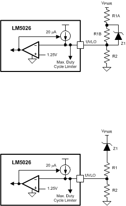 Figure 30. Altering the Slope of Duty Cycle vs VPWR
8.1.9.1 Programmable Maximum Duty Cycle Clamp (DCL)
When the UVLO pin is biased at 1.25 V (minimum operating level), the maximum duty cycle of OUT_A is limited by the duty cycle of the internal clock signal. The duty cycle of the internal clock can be adjusted by programming a voltage set at the DCL pin. The default maximum duty cycle (80%) can be selected by connecting the DCL pin to the RT pin. The DCL pin should not be left open. A small decoupling capacitor located close to the DCL pin is recommended.
The oscillator frequency set resistance (RT) must be determined first before programming the maximum duty cycle. Following the selection of the total RT resistance, the ratio of the RT resistors can be designed to set the desired maximum duty cycle. As the UVLO pin voltage increases from 1.25 V, the maximum duty cycle is reduced by the voltage dependent duty cycle limiter previously as described and shown in Figure 18.
8.2 Typical Application
The following schematic shows an example of an LM5026 controlled 100-W active clamp forward power converter. The input voltage range (VPWR) is 36 V to 78 V, and the output voltage is 3.3 V. The output current capability is 30 Amps. Current sense transformer T2 provides information to the CS pin for current mode control and current limit protection. The error amplifiers and reference U3 and U4 provide voltage feedback through optocoupler U2. Synchronous rectifiers Q3-Q6 minimize rectification losses in the secondary. An auxiliary winding on inductor L2 provides power to the LM5026 VCC pin when the output is in regulation. The input voltage UVLO levels are approximately 34 V for increasing VPWR, and ≈32 V for decreasing VPWR. The circuit can be shut down by forcing the ON/OFF input (J2) below 1.25 V. An external synchronizing frequency can be applied to the SYNC input (J11) or like converters can be self-synchronized by connections of (J3). The regulator output is current limited at approximately 32 A.
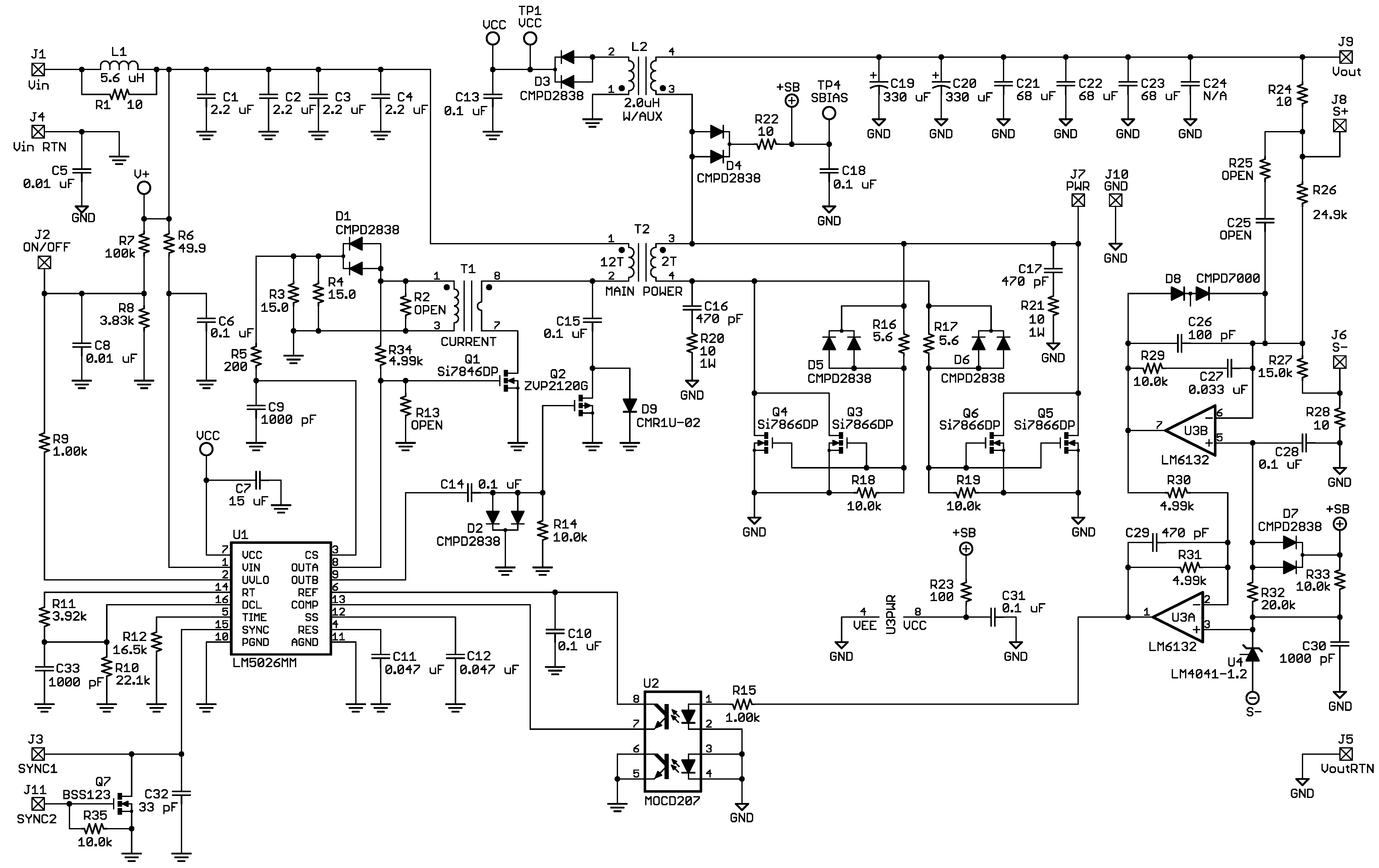 Figure 31. Application Circuit: Input 36 V to 78 V, Output 3.3 V, 30 A
8.2.1 Design Requirements
The design requirements of this application are as follows:
- Input range: 36 V to 78 V
- Output voltage: 3.3 V
- Output current: 0 to 30 A
- Measured efficiency: 90% at 30 A, 92.5% at 15 A
- Frequency of operation: 230 kHz
- Board size: 2.3 × 2.4 × 0.5 inches
- Load Regulation: 1%
- Line Regulation: 0.1%
- Line UVLO, Hiccup Current Limit
8.2.2 Detailed Design Procedure
8.2.2.1 Determine VIN Configuration
First, determine the input voltage range of the application. If the maximum input voltage is less than 100 V, use VIN pin connection in Figure 24. If the maximum input voltage exceeds 100 V, use the configuration shown in Figure 25.
8.2.2.2 Determine UVLO Configuration
As described in Undervoltage Lockout (UVLO), two external resistors program the minimum operational voltage for the power converter. Use Equation 6 and Equation 7 to calculate the resistor values. If remote standby and disable control is needed, use the configuration in Figure 27.
8.2.2.3 Configure Operating Frequency
If internal oscillator is used, use Equation 5 to determine the RT resistor value. If external clock is used, use the configuration in Figure 20.
8.2.2.4 Configure Hiccup Mode and Soft Start
The delay time to restart is programmed with the selection of the RES pin capacitor. Soft-start time is programmed by the capacitor on SS pin. Refer to Hiccup Mode Current Limit Restart (RES) and Equation 8, Equation 9, and Equation 10 to determine the capacitor values.
8.2.2.5 Determine Deadtime and Maximum Duty Cycle
The PWM output phasing the timing is shown in Figure 14. Use Equation 1 and Equation 2 to determine the deadtime programming resistor value. Maximum duty cycle clamp is determined by DCL pin voltage. Use Equation 4 and Figure 17 to determine RT1 and RT2 values.
8.2.3 Application Curves
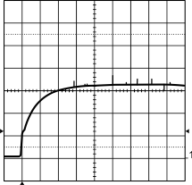
| Input Voltage = 48VDC | ||
| Output Current = 5 A | ||
| Trace 1: Output Voltage V/div = 1 V | ||
| Horizontal Resolution = 1 ms/div |
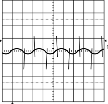
| Input Voltage = 48VDC | ||
| Output Current = 30 A | ||
| Bandwidth Limit = 25 MHz | ||
| Trace 1: Output Voltage V/div = 50 mV | ||
| Horizontal Resolution = 2 µs/div |
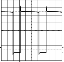
| Input Voltage = 78VDC | ||
| Output Current = 25 A | ||
| Trace 1: Q1 Drain Voltage V/div = 20 V | ||
| Horizontal Resolution = 1 µs/div |
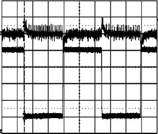
| Input Voltage = 48VDC | ||
| Output Current = 5 A to 25 A | ||
| Trace 1: Output Voltage V/div = 0.5 V | ||
| Trace 2: Output Current, A/div = 5 V | ||
| Horizontal Resolution = 1 ms/div |
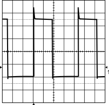
| Input Voltage = 38VDC | ||
| Output Current = 25 A | ||
| Trace 1: Q1 Drain Voltage V/div = 20 V | ||
| Horizontal Resolution = 1 µs/div |
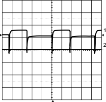
| Input Voltage = 48VDC | ||
| Output Current = 5 A | ||
| Synchronous Rectifier, Q3 Gate V/div = 5 V Trance 1 | ||
| Synchronous Rectifier, Q3 Gate V/div = 5 V Trance 2 | ||
| Synchronous Rectifier, Q5 Gate V/div = 5 V | ||
| Horizontal Resolution = 1 µs/div |