SNVS506J May 2008 – December 2015 LM3691
PRODUCTION DATA.
- 1 Features
- 2 Applications
- 3 Description
- 4 Revision History
- 5 Voltage Options
- 6 Pin Configuration and Functions
- 7 Specifications
- 8 Detailed Description
- 9 Application and Implementation
- 10Power Supply Recommendations
- 11Layout
- 12Device and Documentation Support
- 13Mechanical, Packaging, and Orderable Information
11 Layout
11.1 Layout Guidelines
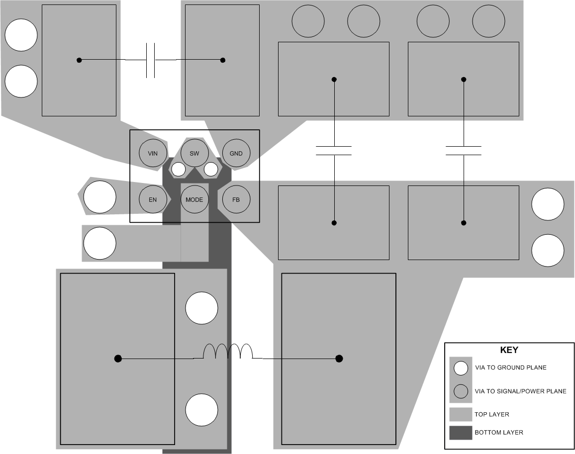
PC board layout is an important part of DC-DC converter design. Poor board layout can disrupt the performance of a DC-DC converter and surrounding circuitry by contributing to EMI, ground bounce, and resistive voltage loss in the traces. These can send erroneous signals to the DC-DC converter device, resulting in poor regulation or instability. In particular parasitic inductance from extra-long PCB trace lengths can cause additional noise voltages through L × di/dt that adversely affect the DC-DC converter device circuitry. Good layout for the LM3691 can be implemented by following a few simple design rules.
- Place the inductor and filter capacitors close together and make the traces short. The traces between these components carry relatively high switching currents and act as antennas. Following this rule reduces radiated noise.
- Place the capacitors and inductor close to the LM3691. Place the CIN capacitor as close to the VIN and GND pads as possible. Place the COUT capacitor as close to the VOUT and GND connections as possible.
- Arrange the components so that the switching current loops curl in the same direction. During the first half of each cycle, current flows from the input filter capacitor, through the buck and inductor to the output filter capacitor and back through ground, forming a current loop. In the second half of each cycle, current is pulled up from ground, through the buck by the inductor, to the output filter capacitor and then back through ground, forming a second current loop. Routing these loops so the current curls in the same direction prevents magnetic field reversal between the two half-cycles and reduces radiated noise.
- Connect the ground pins of the buck and filter capacitors together using generous component-side copper fill as a pseudo-ground plane. Connect this to the ground-plane (if one is used) with several vias. This reduces ground-plane noise by preventing the switching currents from circulating through the ground plane. It also reduces ground bounce at the buck by giving it a low-impedance ground connection.
- Use wide traces between the power components and for power connections to the DC-DC converter circuit. This reduces voltage errors by resistive losses across the traces. Even 1 mm of fine trace creates parasitic inductance that can undesirably affect performance from increased L × di/dt noise voltages.
- Route noise sensitive traces, such as the voltage feedback path, away from noisy traces between the power components. The voltage feedback trace must remain close to the buck circuit, must be routed directly from FB to VOUT at the output capacitor, and must be routed opposite to noise components. This reduces EMI radiated onto the voltage feedback trace of the DC-DC converter.
11.2 Layout Example
 Figure 53. LM3291 Layout Example
11.3 DSBGA Package Assembly and Use
Use of the DSBGA package requires specialized board layout, precision mounting, and careful re-flow techniques, as detailed in TI Application Note DSBGA Wafer Level Chip Scale Package (SNVA009). Refer to the section Surface Mount Assembly Considerations. For best results in assembly, alignment ordinals on the PC board must be used to facilitate placement of the device. The pad style used with DSBGA package must be the NSMD (non-solder mask defined) type. This means that the solder-mask opening is larger than the pad size. This prevents a lip that otherwise forms if the solder-mask and pad overlap, from holding the device off the surface of the board and interfering with mounting. See SNVA009 for specific instructions how to do this.
The 6-pin package used for LM3691 has 300-micron solder balls and requires 10.82 mils pads for mounting on the circuit board. The trace to each pad must enter the pad with a 90° entry angle to prevent debris from being caught in deep corners. Initially, the trace to each pad must be 7-mil wide, for a section approximately 7-mil long or longer, as a thermal relief. Then each trace must neck up or down to its optimal width. The important criteria is symmetry. This ensures the solder bumps on the LM3691 re-flow evenly and that the device solders level to the board. In particular, special attention must be paid to the pads for bumps A2 and C2, because GND and VIN are typically connected to large copper planes.
The DSBGA package is optimized for the smallest possible size in applications with red or infrared opaque cases. Because the DSBGA package lacks the plastic encapsulation characteristic of larger devices, it is vulnerable to light. Backside metallization and/or epoxy coating, along with front side shading by the printed circuit board, reduce this sensitivity. However, the package has exposed die edges. In particular, DSBGA devices are sensitive to light, in the red and infrared range, shining on the exposed die edges of the package.