SNVS506J May 2008 – December 2015 LM3691
PRODUCTION DATA.
- 1 Features
- 2 Applications
- 3 Description
- 4 Revision History
- 5 Voltage Options
- 6 Pin Configuration and Functions
- 7 Specifications
- 8 Detailed Description
- 9 Application and Implementation
- 10Power Supply Recommendations
- 11Layout
- 12Device and Documentation Support
- 13Mechanical, Packaging, and Orderable Information
9 Application and Implementation
NOTE
Information in the following applications sections is not part of the TI component specification, and TI does not warrant its accuracy or completeness. TI’s customers are responsible for determining suitability of components for their purposes. Customers should validate and test their design implementation to confirm system functionality.
9.1 Application Information
The LM3691 step-down DC-DC converter is optimized for powering ultralow-voltage circuits from a single Li-Ion cell (2.7 V to 5.5 V) or 3-cell NiMH/NiCd (2.4 V to 4.5 V) batteries. It provides up to 1-A load current over an input voltage range from 2.3 V to 5.5 V. Seven different fixed voltage output options are available to cover all commonly used voltage rails (0.75 V, 1 V, 1.2 V, 1.5 V, 1.8 V, 2.5 V, 3.3 V).
9.2 Typical Application
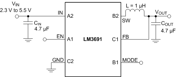 Figure 44. LM3691 Typical Application
9.2.1 Design Requirements
For typical step-down DC-DC applications, use the parameters listed in Table 2.
Table 2. Design Parameters
| DESIGN PARAMETER | EXAMPLE VALUE |
|---|---|
| Minimum input voltage | 2.5 V |
| Minimum output voltage | 1.8 V |
| Output current | 150 mA |
9.2.2 Detailed Design Procedure
9.2.2.1 Inductor Selection
DC bias current characteristics of inductors must be considered. Different manufacturers follow different saturation current rating specifications, so attention must be given to details. DC bias curves should be requested from the manufacturer as part of the inductor selection process.
Minimum value of inductance to specify good performance is 0.5 µH at 1.5 A (ILIM typical) bias current over the ambient temp range. DC resistance of the inductor must be less than 0.1 Ω for good efficiency at high-current condition. The inductor AC loss (resistance) also affects conversion efficiency. Higher Q factor at switching frequency usually gives better efficiency at light load to middle load.
Table 3 lists suggested inductors and suppliers.
Table 3. Suggested Inductors and Their Suppliers
| MODEL | VENDOR | DIMENSIONS L x W x H (mm) | DCR (mΩ) |
|---|---|---|---|
| LQM2HPN1R0MG0 | Murata | 2.5 × 2.0 × 1.0 | 55 |
| MLP2520S1R0L | TDK | 2.5 × 2.0 × 1.0 | 60 |
| KSLI252010BG1R0 | HItachi Metals | 2.5 × 2.0 × 1.0 | 80 |
| MIPSZ2012D1R0 | FDK | 2.0 × 1.25 × 1.0 | 90 |
9.2.2.2 Input Capacitor Selection
A ceramic input capacitor of 4.7 µF, 6.3 V/10 V is sufficient for most applications. Place the input capacitor as close as possible to the VIN pin and GND pin of the device. A larger value or higher voltage rating may be used to improve input voltage filtering. Use X7R, X5R or B types; do not use Y5V or F. DC bias characteristics of ceramic capacitors must be considered when selecting case sizes like 0402. Minimum input capacitance to ensure good performance is 2.2 µF at maximum input voltage DC bias including tolerances and over ambient temperature range.
The input filter capacitor supplies current to the PFET (high-side) switch in the first half of each cycle and reduces voltage ripple imposed on the input power source. A ceramic capacitor's low ESR provides the best noise filtering of the input voltage spikes due to this rapidly changing current. Select an input filter capacitor with sufficient ripple current rating. The input current ripple can be calculated as:

9.2.2.3 Output Capacitor Selection
Use a 4.7-μF, 6.3-V ceramic capacitor, X7R, X5R or B types; do not use Y5V or F. DC bias voltage characteristics of ceramic capacitors must be considered. DC bias characteristics vary from manufacturer to manufacturer, and DC bias curves should be requested from the manufacturer as part of the capacitor selection process. The output filter capacitor smooths out current flow from the inductor to the load, helps maintain a steady output voltage during transient load changes, and reduces output voltage ripple. These capacitors must be selected with sufficient capacitance and sufficiently low equivalent series resistance (ESR) to perform these functions. Minimum output capacitance to specify good performance is 2.2 µF at the output voltage DC bias including tolerances and over ambient temperature range.
The output voltage ripple is caused by the charging and discharging of the output capacitor and also due to its RESR and can be calculated as:
Voltage peak-to-peak ripple due to capacitance is shown in Equation 2:

Voltage peak-to-peak ripple due to ESR Equation 3:
Because these two components are out of phase the RMS value can be used to get an approximate value of peak-to-peak ripple.
Voltage peak-to-peak ripple, root mean squared equals:

Note that the output voltage ripple is dependent on the current ripple and the ESR of the output capacitor (RESR). The RESR is frequency dependent (as well as temperature dependent); make sure the value used for calculations is at the switching frequency of the part.
Table 4 lists suggested capacitors and suppliers.
Table 4. Suggested Capacitors and Their Suppliers
| MODEL | TYPE | VENDOR | VOLTAGE RATING (V) | CASE SIZE INCH (mm) |
|---|---|---|---|---|
| 4.7 µF for CIN and COUT | ||||
| C1608X5R0J475K | Ceramic | TDK | 6.3 | 0603 (1608) |
| C1608X5R1A475K | Ceramic | TDK | 10.0 | 0603 (1608) |
9.2.3 Application Curves
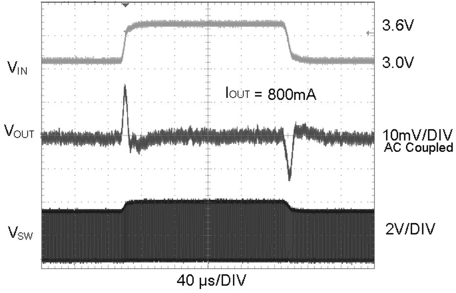
| VOUT = 1.8 V |
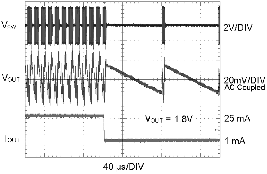
| VOUT = 1.8 V | ECO Mode 25 mA to 1 mA | |
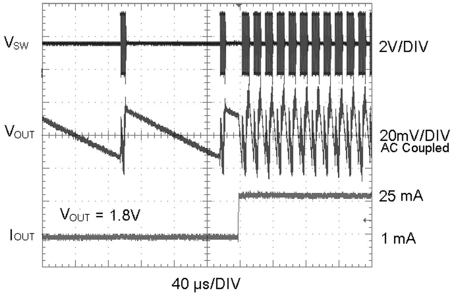
| VOUT = 1.8 V | ECO Mode 1 mA to 25 mA | |
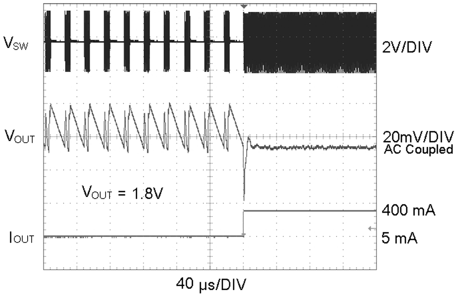
| VOUT = 1.8 V | ECO Mode to PWM Mode | |
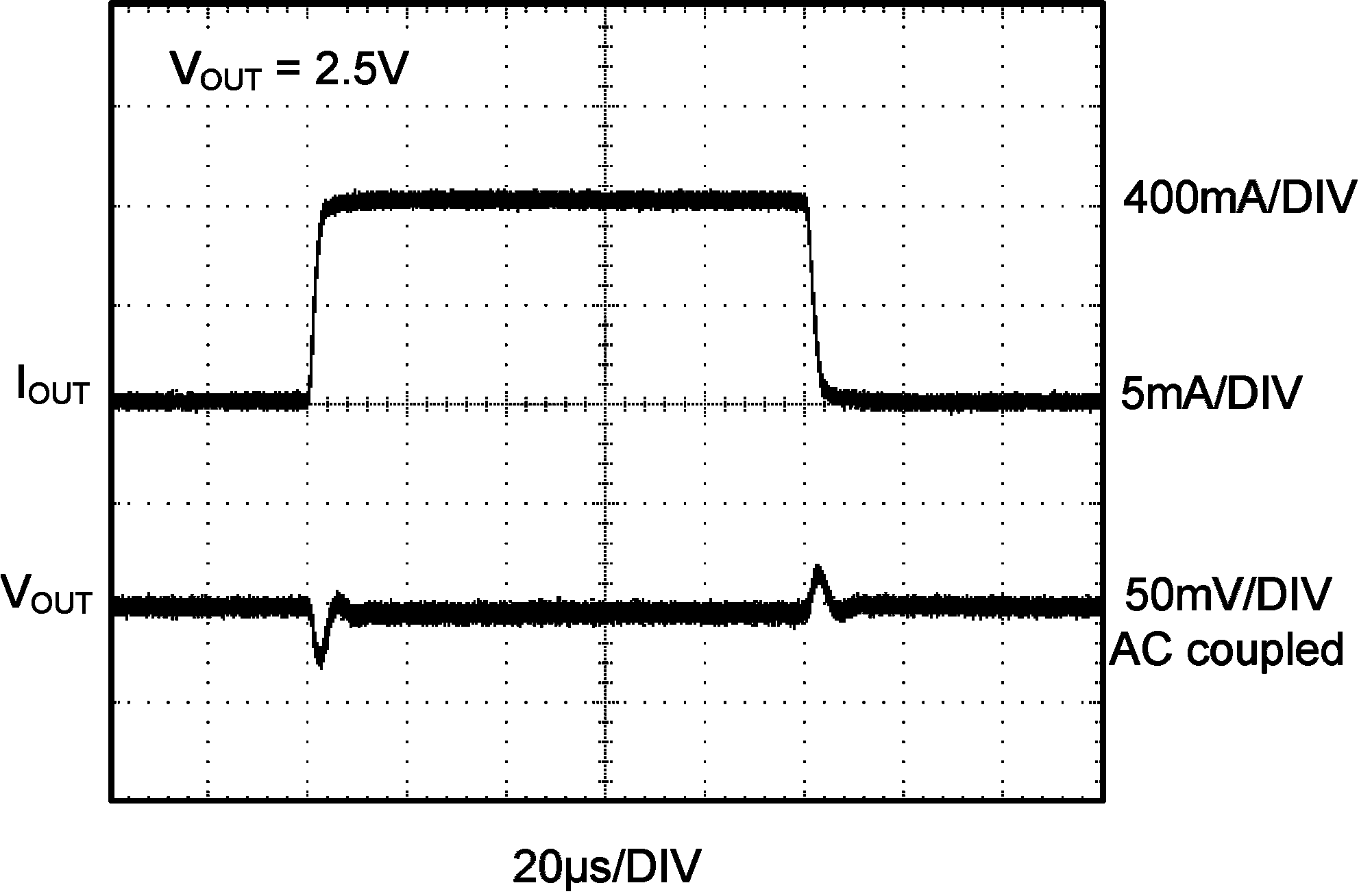
| VOUT = 1.8 V | FPWM Mode |
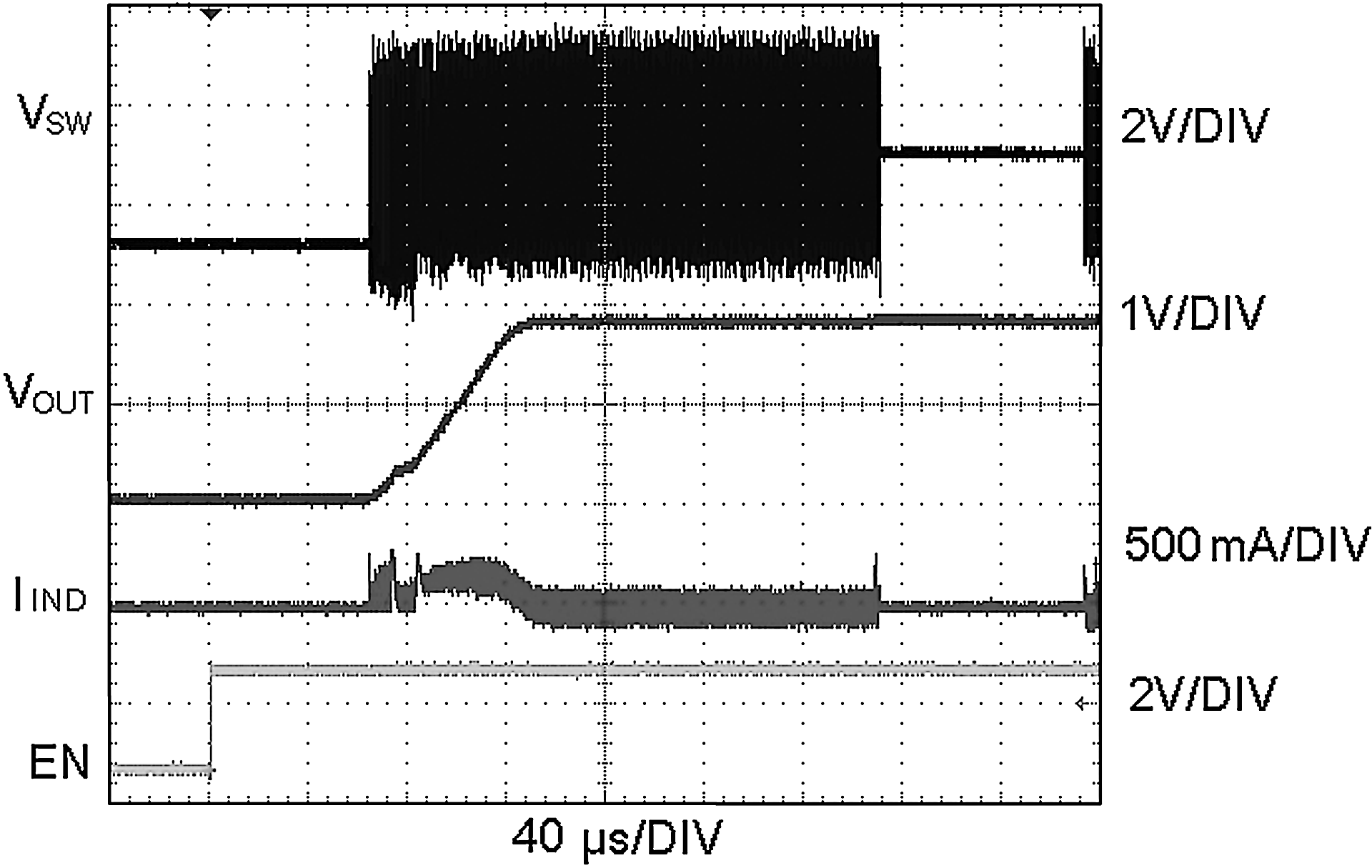
| VOUT = 1.8 V | ROUT = 1.8 kΩ |

| VOUT = 1.8 V | FPWM Mode |
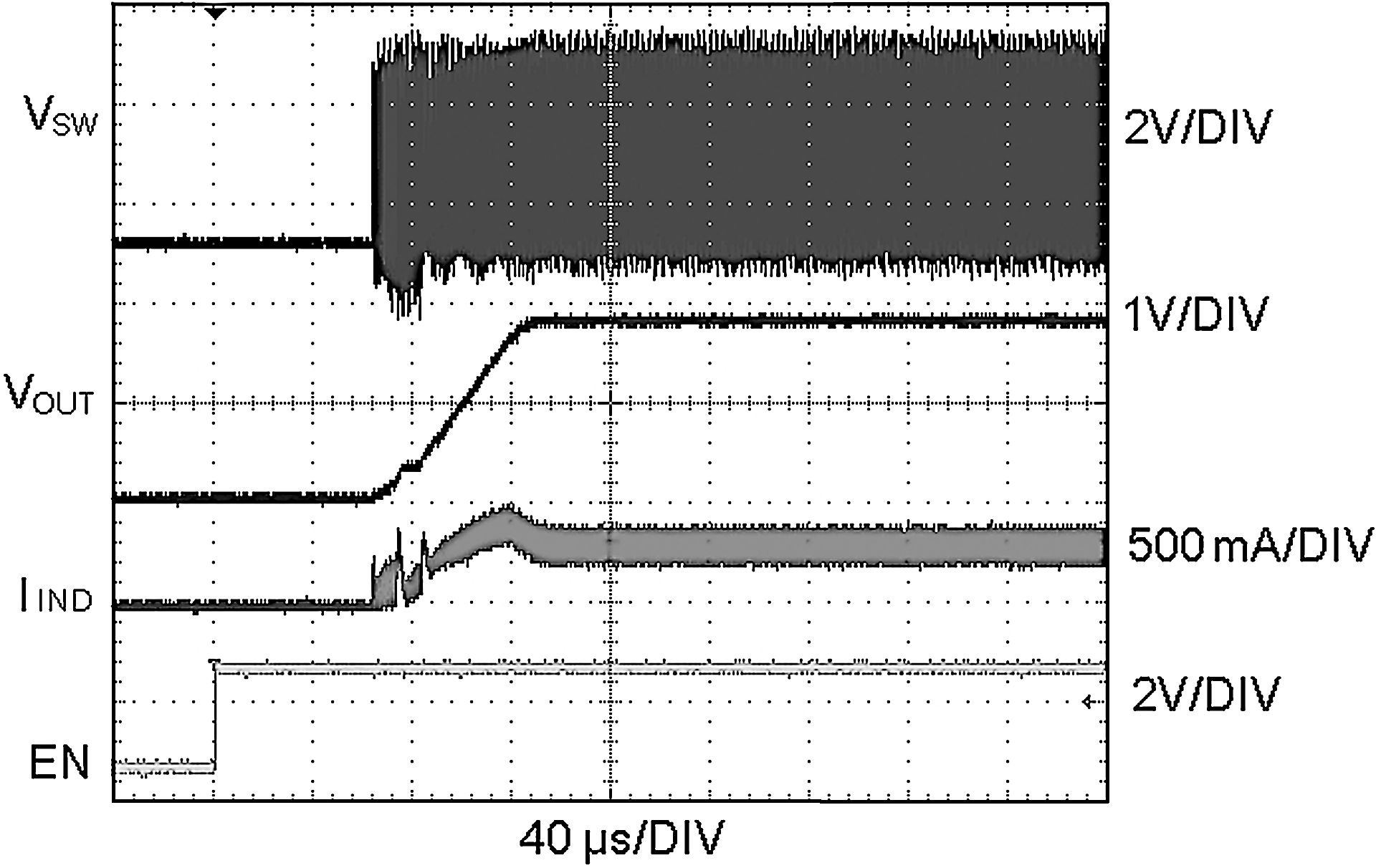
| VOUT = 1.8 V | ROUT = 6 Ω |