SNVS239C October 2004 – October 2015 LM3475
PRODUCTION DATA.
- 1 Features
- 2 Applications
- 3 Description
- 4 Revision History
- 5 Pin Configuration and Functions
- 6 Specifications
- 7 Detailed Description
-
8 Application and Implementation
- 8.1 Application Information
- 8.2
Typical Application
- 8.2.1 Design Requirements
- 8.2.2
Detailed Design Procedure
- 8.2.2.1 Setting Output Voltage
- 8.2.2.2 Setting Operating Frequency and Output Ripple
- 8.2.2.3 Using a Feed-forward Capacitor
- 8.2.2.4 Inductor Selection
- 8.2.2.5 Output Capacitor Selection
- 8.2.2.6 Input Capacitor Selection
- 8.2.2.7 Diode Selection
- 8.2.2.8 P-Channel MOSFET Selection
- 8.2.2.9 Reducing Switching Noise
- 8.2.3 Application Curves
- 9 Power Supply Recommendations
- 10Layout
- 11Device and Documentation Support
- 12Mechanical, Packaging, and Orderable Information
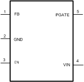
5 Pin Configuration and Functions
DBV Package
5-Pin SOT-23
Top View

Pin Functions
| PIN | I/O | DESCRIPTION | |
|---|---|---|---|
| NAME | NO. | ||
| FB | 1 | I | Feedback input. Connect to a resistor divider between the output and GND. |
| GND | 2 | G | Ground. |
| EN | 3 | O | Enable. Pull this pin above 1.5 V (typical) for normal operation. When EN is low, the device enters shutdown mode. |
| VIN | 4 | P | Power supply input. |
| PGATE | 5 | O | Gate drive output for the external PFET. |