SNVS239C October 2004 – October 2015 LM3475
PRODUCTION DATA.
- 1 Features
- 2 Applications
- 3 Description
- 4 Revision History
- 5 Pin Configuration and Functions
- 6 Specifications
- 7 Detailed Description
-
8 Application and Implementation
- 8.1 Application Information
- 8.2
Typical Application
- 8.2.1 Design Requirements
- 8.2.2
Detailed Design Procedure
- 8.2.2.1 Setting Output Voltage
- 8.2.2.2 Setting Operating Frequency and Output Ripple
- 8.2.2.3 Using a Feed-forward Capacitor
- 8.2.2.4 Inductor Selection
- 8.2.2.5 Output Capacitor Selection
- 8.2.2.6 Input Capacitor Selection
- 8.2.2.7 Diode Selection
- 8.2.2.8 P-Channel MOSFET Selection
- 8.2.2.9 Reducing Switching Noise
- 8.2.3 Application Curves
- 9 Power Supply Recommendations
- 10Layout
- 11Device and Documentation Support
- 12Mechanical, Packaging, and Orderable Information
7 Detailed Description
7.1 Overview
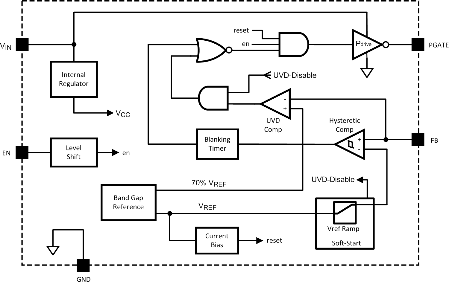
The LM3475 is a buck (step-down) DC-DC controller that uses a hysteretic control architecture, which results in Pulse Frequency Modulated (PFM) regulation. The hysteretic control scheme does not utilize an internal oscillator. Switching frequency depends on external components and operating conditions. Operating frequency decreases at light loads, resulting in excellent efficiency compared to PWM architectures. Because switching is directly controlled by the output conditions, hysteretic control provides exceptional load transient response.
7.2 Functional Block Diagram

7.3 Feature Description
7.3.1 Hysteretic Control Circuit
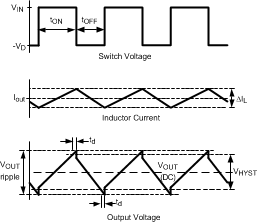
The LM3475 uses a comparator-based voltage control loop. The voltage on the feedback pin is compared to a 0.8V reference with 21mV of hysteresis. When the FB input to the comparator falls below the reference voltage, the output of the comparator goes low. This results in the driver output, PGATE, pulling the gate of the PFET low and turning on the PFET.
With the PFET on, the input supply charges COUT and supplies current to the load through the PFET and the inductor. Current through the inductor ramps up linearly, and the output voltage increases. As the FB voltage reaches the upper threshold (reference voltage plus hysteresis) the output of the comparator goes high, and the PGATE turns the PFET off. When the PFET turns off, the catch diode turns on, and the current through the inductor ramps down. As the output voltage falls below the reference voltage, the cycle repeats. The resulting output, inductor current, and switch node waveforms are shown in Figure 9.
 Figure 9. Hysteretic Waveforms
7.3.2 Soft-Start
The LM3475 includes an internal soft-start function to protect components from excessive inrush current and output voltage overshoot. As VIN rises above 2.7 V (typical), the internal bias circuitry becomes active. When EN goes high, the device enters soft-start. During soft-start, the reference voltage is ramped up to the nominal value of 0.8 V in approximately 4ms. Duty cycle and output voltage will increase as the reference voltage is ramped up.
7.3.3 Under Voltage Detection
When the output voltage falls below 70% (typical) of the normal voltage, as measured at the FB pin, the device turns off PFET and restarts a new soft-start cycle. In short circuit, the PFET is always on, and the converter is effectively a resistor divider from input to output to ground. Whether the part restarts depends on the power path resistance and the short circuit resistance. This feature should not be considered as overcurrent protection or output short circuit protection.
7.3.4 PGATE
During switching, the PGATE pin swings from VIN (off) to ground (on). As input voltage increases, the time it takes to slew the gate of the PFET on and off also increases. Also, as the PFET gate voltage approaches VIN, the PGATE current driving capability decreases. This can cause a significant additional delay in turning the switch off when using a PFET with a low threshold voltage. These two effects will increase power dissipation and reduce efficiency. Therefore, a PFET with relatively high threshold voltage and low gate capacitance is recommended.
7.3.5 Minimum On or Off Time
To ensure accurate comparator switching, the LM3475 imposes a blanking time after each comparator state change. This blanking time is 180 ns typically. Immediately after the comparator goes high or low, it will be held in that state for the duration of the blanking time. This helps keep the hysteretic comparator from improperly responding to switching noise spikes (See Reducing Switching Noise) and ESL spikes (See Output Capacitor Selection) at the output.
At very low or very high duty cycle operation, maximum frequency will be limited by the blanking time. The maximum operating frequency can be determined by the following equations:
where
- D is the duty cycle, defined as VOUT/VIN, and tonmin
- toffmin is the sum of the blanking time, the propagation delay time, and the PFET delay time (see Figure 9)
7.3.6 Enable Pin (EN)
The LM3475 provides a shutdown function via the EN pin to disable the device. The device is active when the EN pin is pulled above 1.5 V (typ) and in shutdown mode when EN is below 1.135 V (typ). In shutdown mode, total quiescent current is less than 10 µA. The EN pin can be directly connected to VIN for always-on operation.
7.4 Device Functional Modes
The LM3475 operates in discontinuous conduction mode at light load current and continuous conduction mode at heavy load current. In discontinuous conduction mode, current through the inductor starts at zero and ramps up to the peak, then ramps down to zero. The next cycle starts when the FB voltage reaches the reference voltage. Until then, the inductor current remains zero. Operating frequency is low, as are switching losses. In continuous conduction mode, current always flows through the inductor and never ramps down to zero.