ZHCSAP9E October 2011 – August 2015 LM3242
PRODUCTION DATA.
6 Specifications
6.1 Absolute Maximum Ratings
over operating free-air temperature range (unless otherwise noted)(1)| MIN | MAX | UNIT | ||
|---|---|---|---|---|
| VIN to SGND | −0.2 | 6 | V | |
| PGND to SGND | −0.2 | 0.2 | V | |
| EN, VCON, BPEN | (SGND − 0.2) | (VIN + 0.2) w/ 6 V | V | |
| SW, FB | (PGND – 0.2) | (VIN + 0.2) | V | |
| Continuous power dissipation(2) | Internally limited | |||
| Maximum lead temperature (soldering, 10 sec) | 260 | °C | ||
| Junction temperature, TJ-MAX | 150 | °C | ||
| Storage temperature, Tstg | −65 | 150 | °C | |
(1) Stresses beyond those listed under Absolute Maximum Ratings may cause permanent damage to the device. These are stress ratings only, which do not imply functional operation of the device at these or any other conditions beyond those indicated under Recommended Operating Conditions. Exposure to absolute-maximum-rated conditions for extended periods may affect device reliability.
(2) Internal thermal shutdown circuitry protects the device from permanent damage. Thermal shutdown engages at TJ = 150°C (typical) and disengages at TJ = 125°C (typical).
6.2 ESD Ratings
| VALUE | UNIT | |||
|---|---|---|---|---|
| V(ESD) | Electrostatic discharge | Human-body model (HBM), per ANSI/ESDA/JEDEC JS-001(1) | ±2000 | V |
| Charged-device model (CDM), per JEDEC specification JESD22-C101(2) | ±1250 | |||
| Machine model | ±200 | |||
(1) JEDEC document JEP155 states that 500-V HBM allows safe manufacturing with a standard ESD control process.
(2) JEDEC document JEP157 states that 250-V CDM allows safe manufacturing with a standard ESD control process.
6.3 Recommended Operating Conditions
over operating free-air temperature range (unless otherwise noted)(1)| MIN | NOM | MAX | UNIT | ||
|---|---|---|---|---|---|
| Input voltage | 2.7 | 5.5 | V | ||
| Recommended load current | 0 | 750 | mA | ||
| PWM mode | 0 | 750 | mA | ||
| Bypass mode | 0 | 1000 | mA | ||
| Junction temperature, TJ | −30 | 125 | °C | ||
| Ambient temperature, TA(2) | −30 | 90 | °C | ||
(1) All voltages are with respect to the potential at the GND pins.
(2) In applications where high power dissipation and/or poor package thermal resistance is present, the maximum ambient temperature may have to be de-rated. Maximum ambient temperature (TA-MAX) is dependent on the maximum operating junction temperature (TJ-MAX-OP = 125°C), the maximum power dissipation of the device in the application (PD-MAX), and the junction-to ambient thermal resistance of the part/package in the application (RθJA), as given by the following equation: TA-MAX = TJ-MAX-OP – (RθJA × PD-MAX).
6.4 Thermal Information
| THERMAL METRIC(1) | LM3242 | UNIT | |
|---|---|---|---|
| YFQ (DSBGA) | |||
| 9 PINS | |||
| RθJA | Junction-to-ambient thermal resistance | 85 | °C/W |
(1) For more information about traditional and new thermal metrics, see the Semiconductor and IC Package Thermal Metrics application report, SPRA953.
6.5 Electrical Characteristics
All typical limits in are for TA = TJ = 25°C; all minimum and maximum limits apply over the full operating ambient temperature range (−30°C ≤ TA = TJ ≤ +90°C). Unless otherwise noted, all specifications apply to the 典型应用 with VIN = EN = 3.6 V, and BPEN = NC = 0 V.| PARAMETER | TEST CONDITIONS | MIN | TYP | MAX | UNIT | |
|---|---|---|---|---|---|---|
| VFB,MIN | Feedback voltage at minimum setting | PWM mode, VCON = 0.16 V(1) | 0.38 | 0.4 | 0.42 | V |
| VFB,MAX | Feedback voltage at maximum setting | PWM mode, VCON = 1.44 V, VIN = 4 V | 3.55 | 3.6 | 3.65 | V |
| ISHDN | Shutdown supply current | EN = SW = VCON = FB = BPEN = NC = 0 V(2) | 0.1 | 1 | µA | |
| IQ_PWM | PWM mode quiescent current | PWM mode, No switching VCON = 0.13 V, FB = 1 V(3) |
650 | 795 | µA | |
| IQ_SLEEP | Low-power SLEEP mode | EN = VIN, BPEN = NC = 0 V, SW = TriState VCON < 0.08 V(3) |
60 | 80 | µA | |
| IQ_ECO | ECO mode Quiescent current | ECO mode, No switching VCON = 0.8 V, FB = 2.05 V(3) |
60 | 80 | µA | |
| RDSON (P) | Pin-pin resistance for PFET | VIN = VGS = 3.6 V, ISW = 200 mA | 170 | 260 | mΩ | |
| RDSON (N) | Pin-pin resistance for NFET | VIN = VGS = 3.6 V, ISW = −200 mA | 110 | 200 | mΩ | |
| RDSON (BP) | Pin-Pin resistance for BPFET | VIN = VGS = 3.1 V, ISW = −200 mA | 80 | 110 | mΩ | |
| ILIM P | PFET switch peak current limit | See(4) | 1300 | 1450 | 1600 | mA |
| ILIM BP | BPFET switch peak current limit | VFB = VIN − 1 V(4) | 310 | 400 | mA | |
| FOSC | Internal oscillator frequency | 5.7 | 6 | 6.3 | MHz | |
| VIH | EN, BPEN logic high input threshold | 1.2 | V | |||
| VIL | EN, BPEN logic low input threshold | 0.4 | V | |||
| Gain | VCON to VOUT gain | 0.16 V ≤ VCON ≤ 1.44 V(5) | 2.5 | V/V | ||
| IVCON | VCON pin leakage current | VCON = 1 V | ±1 | µA | ||
| VBP,NEG | Auto bypass detection negative threshold | VCON = 1.2 V (VOUT-SET = 3 V) VIN = 3.2 V, RL = 6 Ω, IOUT = 500 mA(6) |
165 | 200 | 235 | mV |
| VBP,POS | Auto bypass detection positive threshold | VCON = 1.2 V (VOUT-SET = 3 V) VIN = 3.25 V, RL = 6 Ω, IOUT = 500 mA(7) |
215 | 250 | 285 | mV |
| IBP,SLEW | Auto bypass IOUT slew current | BPEN = High, Forced bypass | 1600 | mA | ||
(1) All 0.4-V VOUT specifications are at steady-state only.
(2) Shutdown current includes leakage current of PFET.
(3) IQ specified here is when the part is not switching under test mode conditions. For operating quiescent current at no load, refer to Typical Characteristics.
(4) Current limit is built-in, fixed, and not adjustable.
(5) Care must be taken to keep the VCON pin voltage less than the VIN pin voltage as this can place the part into a manufacturing test mode.
(6) Entering Bypass mode VIN is compared to the programmed output voltage (2.5 × VCON). When VIN − (2.5 × VCON) falls below VBP,NEG longer than TBP,NEG, the Bypass FET turns on, and the switching FET turns on.
(7) Bypass mode is exited when VIN − (2.5 × VCON) exceeds VBP,POS longer than TBP,POS, and PWM mode resumes. The hysteresis for the bypass detection threshold VBP,POS – VBP,NEG is always positive and will be approximately 50 mV.
6.6 System Characteristics
The following spec table entries are ensured by design providing the component values in the 典型应用 are used. These parameters are not ensured by production testing. Minimum and Maximum values apply over the full operating ambient temperature range (−30°C ≤ TA ≤ +90°C) and over the VIN range = 2.7 V to 5.5 V unless otherwise specified. L = 0.5 µH, DCR = 50 mΩ, CIN = 10 µF, 6.3 V, 0603 (1608), COUT = 4.7 µF, 6.3 V, 0402.| PARAMETER | TEST CONDITIONS | MIN | TYP | MAX | UNIT | |
|---|---|---|---|---|---|---|
| D | Maximum duty cycle | 100% | ||||
| RBP | Bypass mode resistance(1) | VIN = VGS = 3.1 V, IOUT = –500 mA VCON > 1.16 V |
75 | mΩ | ||
| IOUT | Maximum output current capability | 2.7 V ≤ VIN ≤ 5.5 V 2.5 × VCON ≤ VIN − 285 mV |
750 | mA | ||
| 2.7 V ≤ VIN ≤ 5.5 V 2.5 × VCON ≥ VIN – 165 mV, Bypass mode |
1000 | |||||
| CVCON | VCON input capacitance | VCON = 1 V, Test frequency = 100 KHz | < 1 | pF | ||
| VOUT Linearity | VCON range 0.16 V to 1.44 V | 0 mA ≤ IOUT ≤ 750 mA(2) | −3% | 3% | ||
| −50 | 50 | mV | ||||
| η | Efficiency | VIN = 3.6 V, VOUT = 0.8 V IOUT = 10 mA, ECO mode |
75% | |||
| VIN = 3.6 V, VOUT = 1.8 V IOUT = 200 mA, PWM mode |
90% | |||||
| VIN = 3.9 V, VOUT = 3.3 V IOUT = 500 mA, PWM mode |
95% | |||||
| LINE TR | Line transient response | VIN = 3.6 V to 4.2 V, TR = TF = 10 µs, IOUT = 100 mA, VOUT = 0.8V |
50 | mVpk | ||
| LOAD TR | Load transient response | VIN = 3.1 V/3.6 V/4.5 V, VOUT = 0.8 V, IOUT = 50 mA to 150 mA TR = TF = 0.1 µs |
50 | mVpk | ||
(1) Total resistance in Bypass mode. Total includes the Bypass FET resistance in parallel with the PWM switch path resistance (PFET resistance and series inductor parasistic resistance.)
(2) Linearity limits are ±3% or ±50 mV, whichever is larger. VOUT is monotonic in nature with respect to VCON input.
6.7 Timing Requirements
| MIN | NOM | MAX | UNIT | ||
|---|---|---|---|---|---|
| TVCON_TR | VOUT rise time, VCON change to 90% VIN = 3.7 V, VOUT = 1.4 V to 3.4 V 0.1 µs < VCON_TR < 1 µs, RL = 12 Ω |
9 | µs | ||
| VOUT fall time VCON change to 10% VIN = 3.7 V, VOUT = 3.4 V to 1.4 V 0.1 µs < VCON_TF < 1 µs, RL = 12 Ω |
9 | µs | |||
| TON | Turnon time (time for output to reach 95% final value after Enable low-to-high transition) EN = Low-to-High, VIN = 4.2 V, VOUT = 3.4 V IOUT = < 1 mA, COUT = 4.7 µF |
50(1) | µs | ||
| TBP, NEG | Auto bypass detect negative threshold delay time(2) | 10 | µs | ||
| TBP, POS | Auto bypass detect positive threshold delay time(3) | 0.1 | µs | ||
(1) This parameter is not production-limit tested.
(2) Entering Bypass mode VIN is compared to the programmed output voltage (2.5 × VCON). When VIN − (2.5 × VCON) falls below VBP,NEG longer than TBP,NEG, the Bypass FET turns on, and the switching FET turns on.
(3) Bypass mode is exited when VIN − (2.5 × VCON) exceeds VBP,POS longer than TBP,POS, and PWM mode resumes. The hysteresis for the bypass detection threshold VBP,POS – VBP,NEG is always be positive and will be approximately 50 mV.
6.8 Typical Characteristics
VIN = EN = 3.6 V, L = 0.5 µH, CIN = 10 µF, COUT = 4.7 µF and TA = 25°C, unless otherwise noted.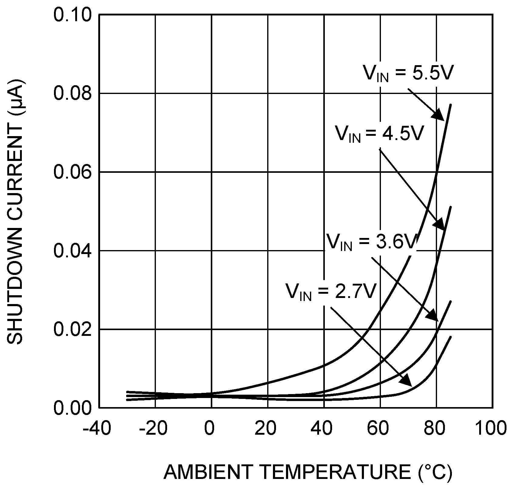
| SW = VCON = EN = 0 V | ||
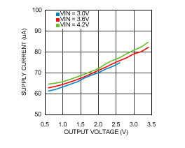
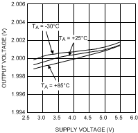
| VOUT = 2 V | RLOAD=10 Ω | |
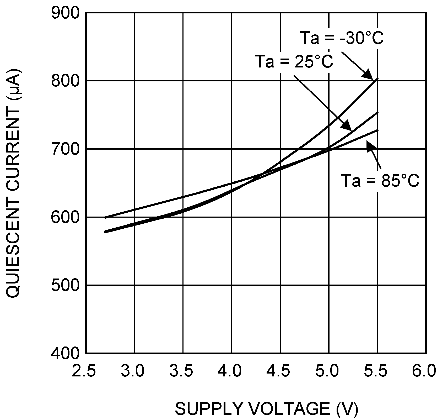
| FB = 1 V | VCON = 0.13 V | |
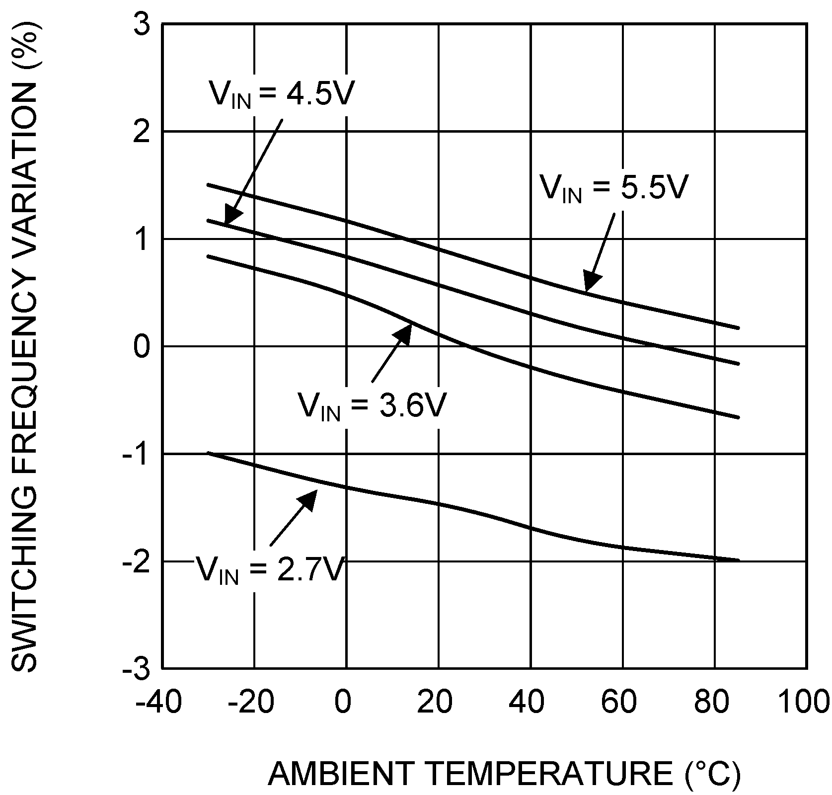
| VOUT = 2 V | IOUT = 200 mA | |
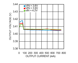
| VOUT = 3.4 V | ||
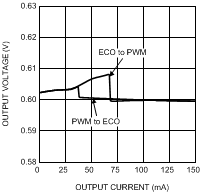
| VOUT = 0.6 V | ||
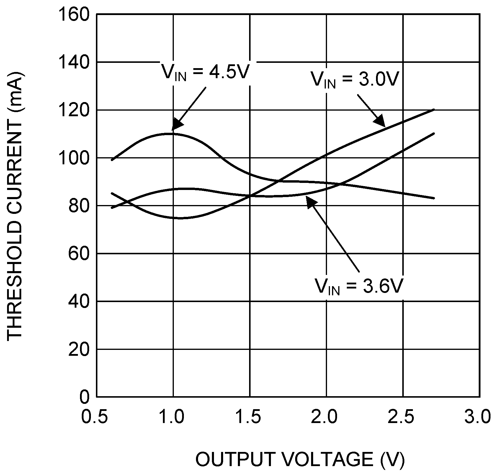
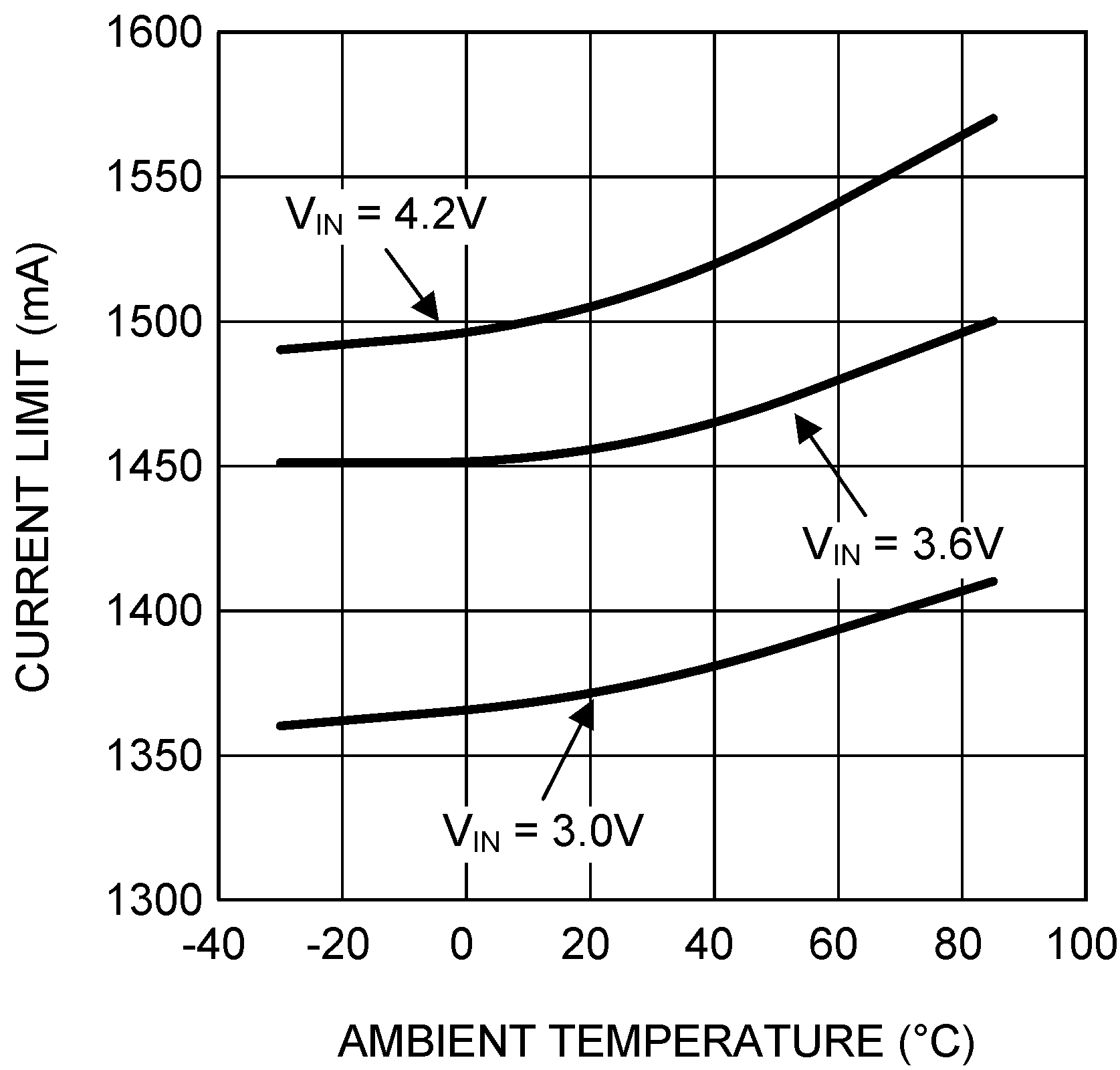
| VOUT = 2 V | ||
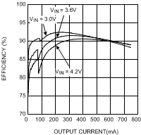
| VOUT = 2 V | ||
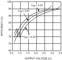
| RLOAD = 10 Ω | ||
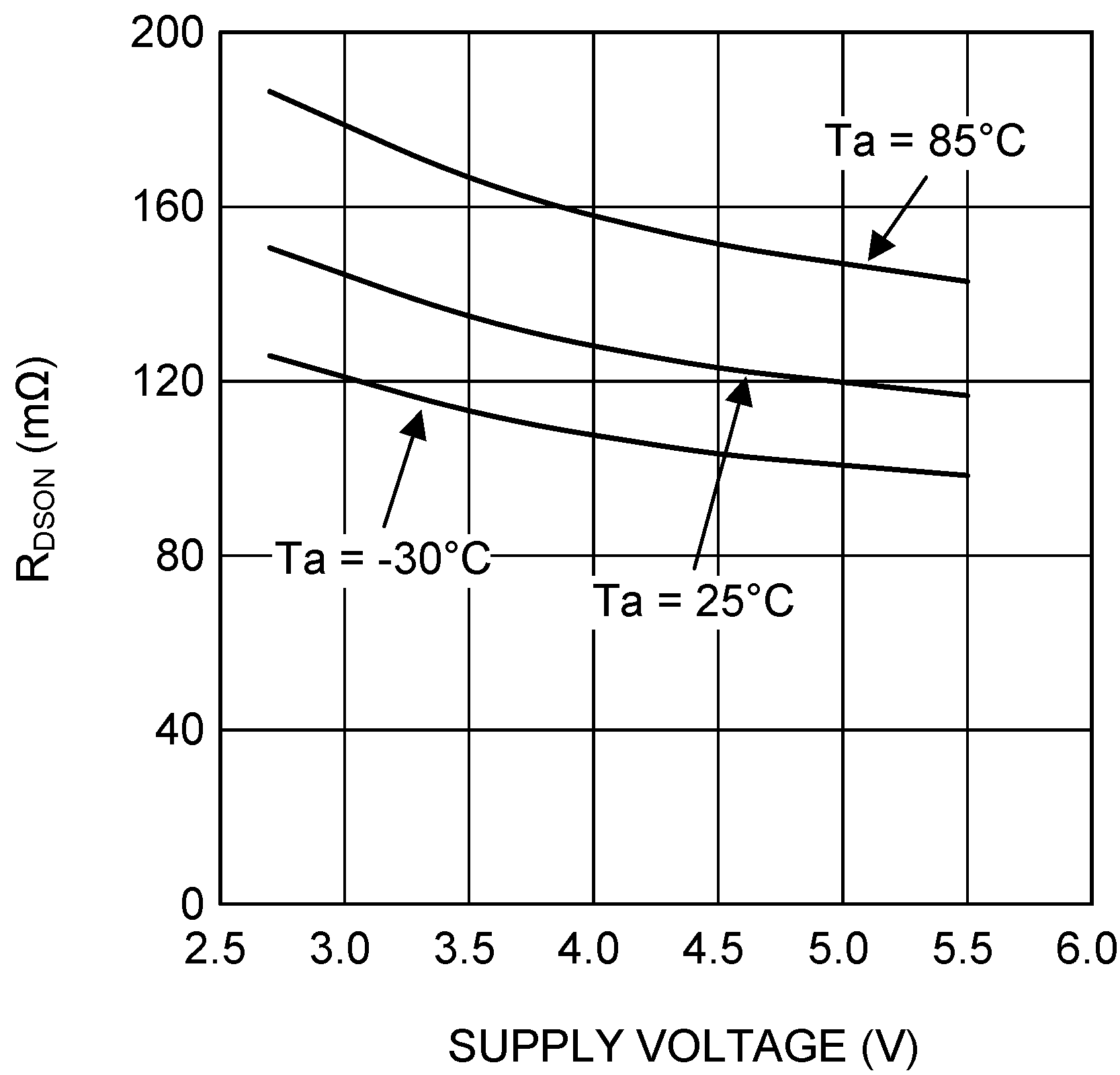
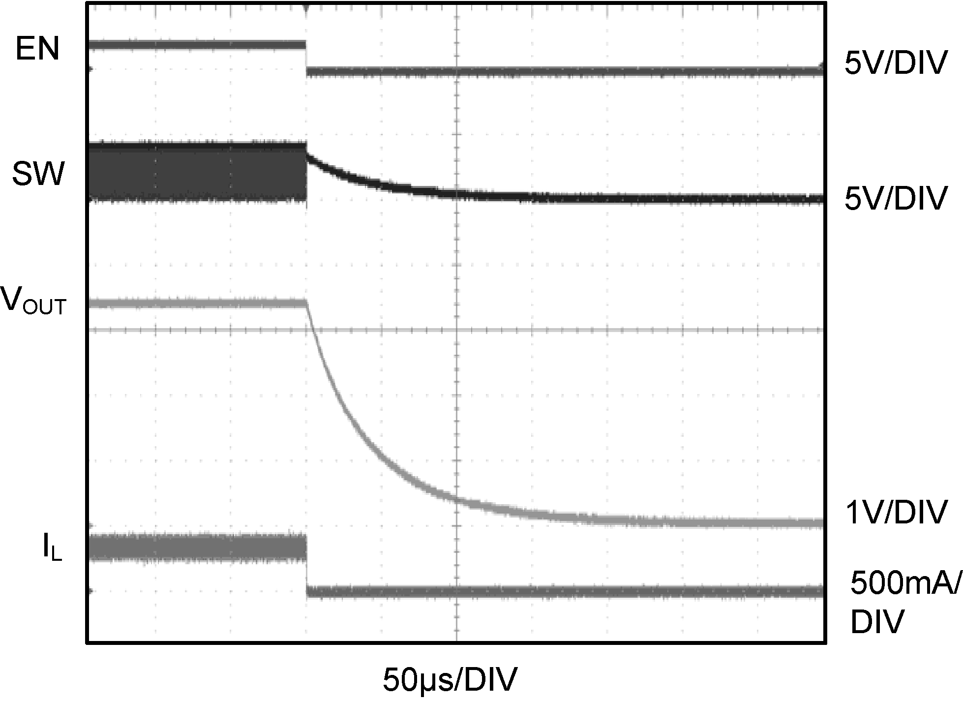
| VIN = 4.2 V | VOUT = 3.4 V | RLOAD =10 Ω |
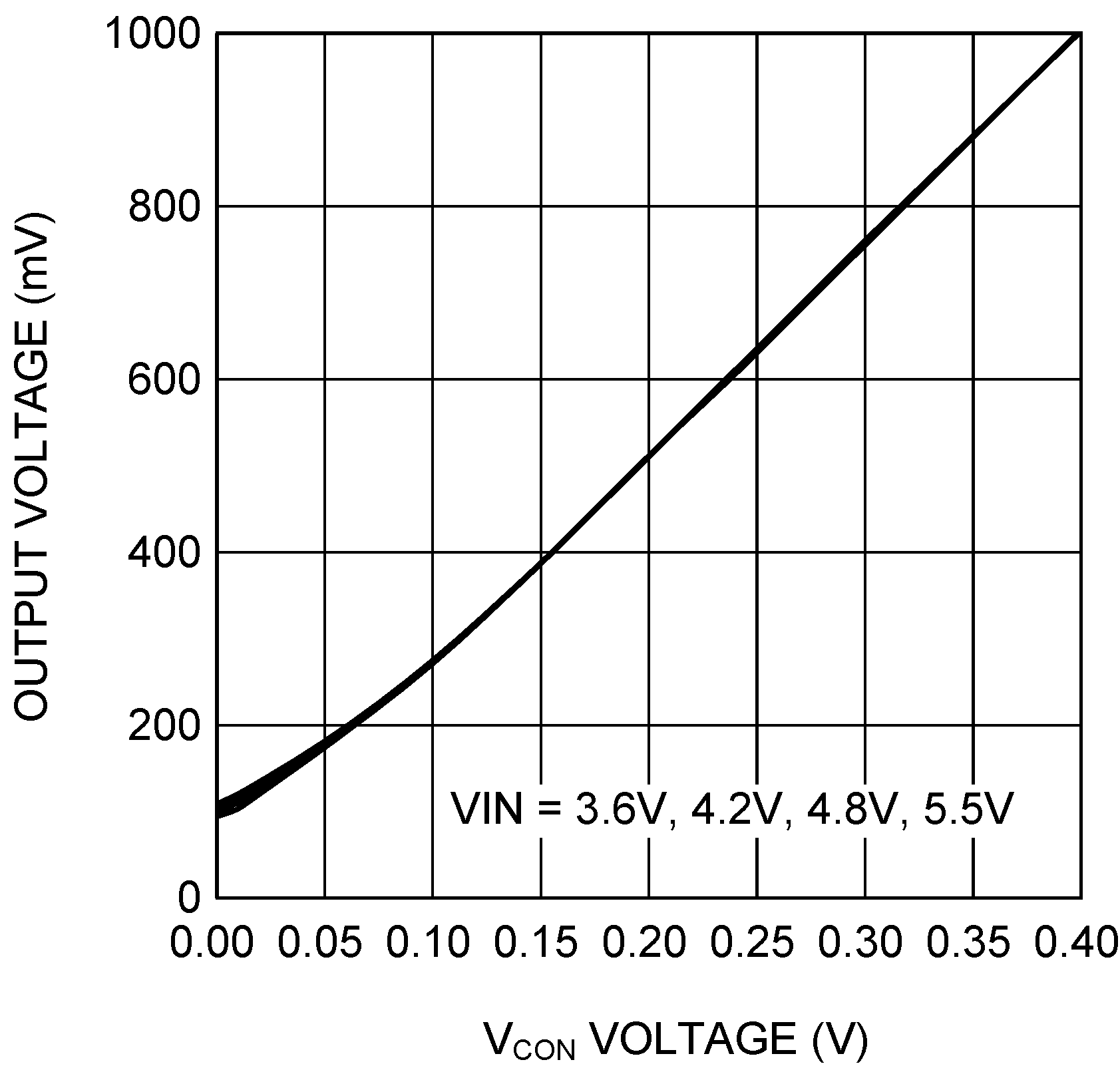
| RLOAD = 10 Ω | ||
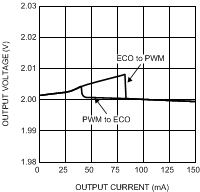
| VOUT = 2 V | ||
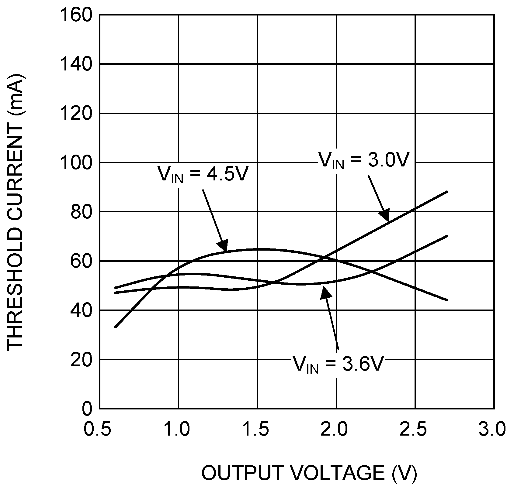
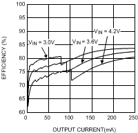
| VOUT = 0.8 V | ||
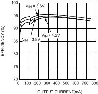
| VOUT = 3.3 V | ||
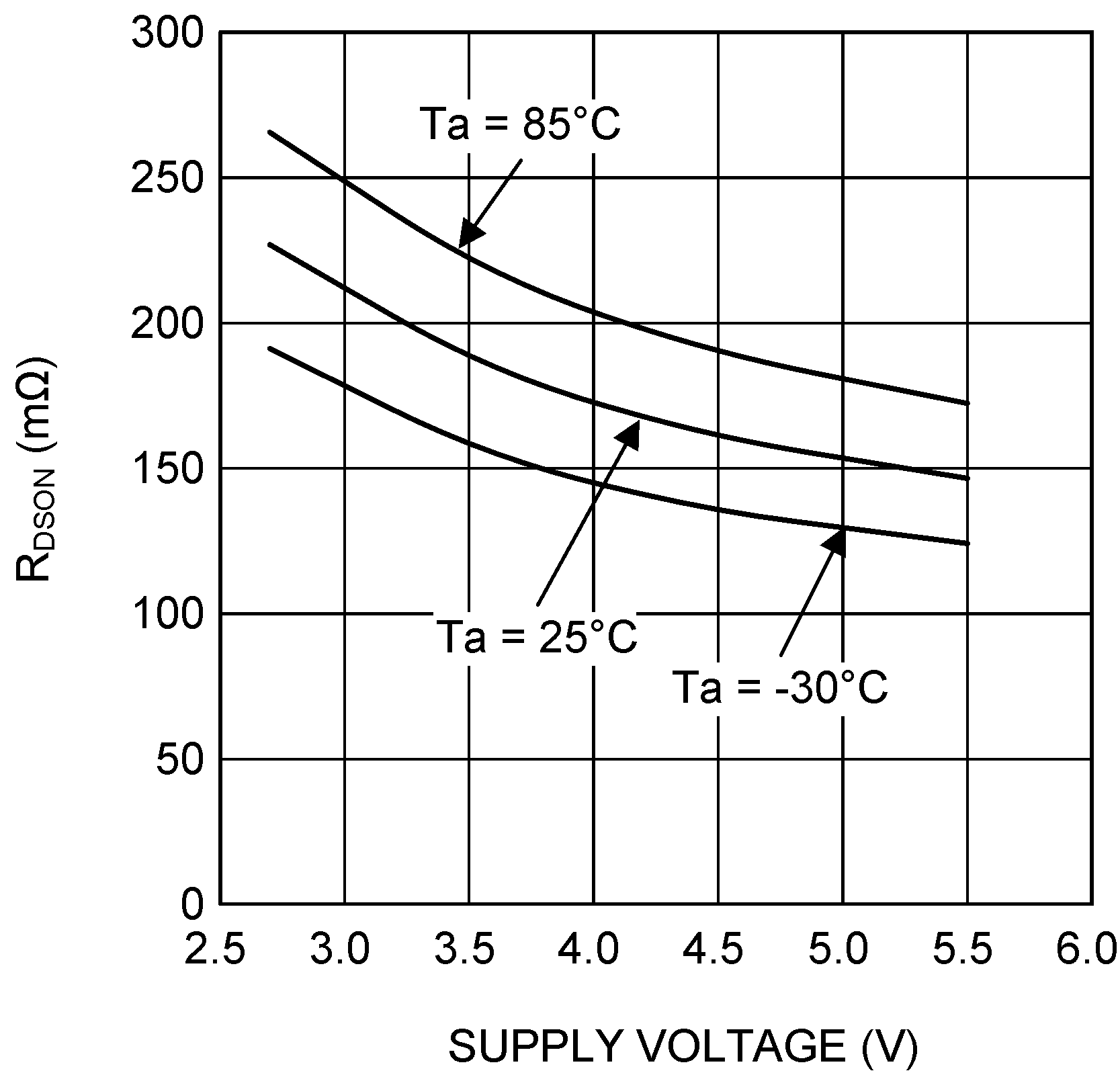
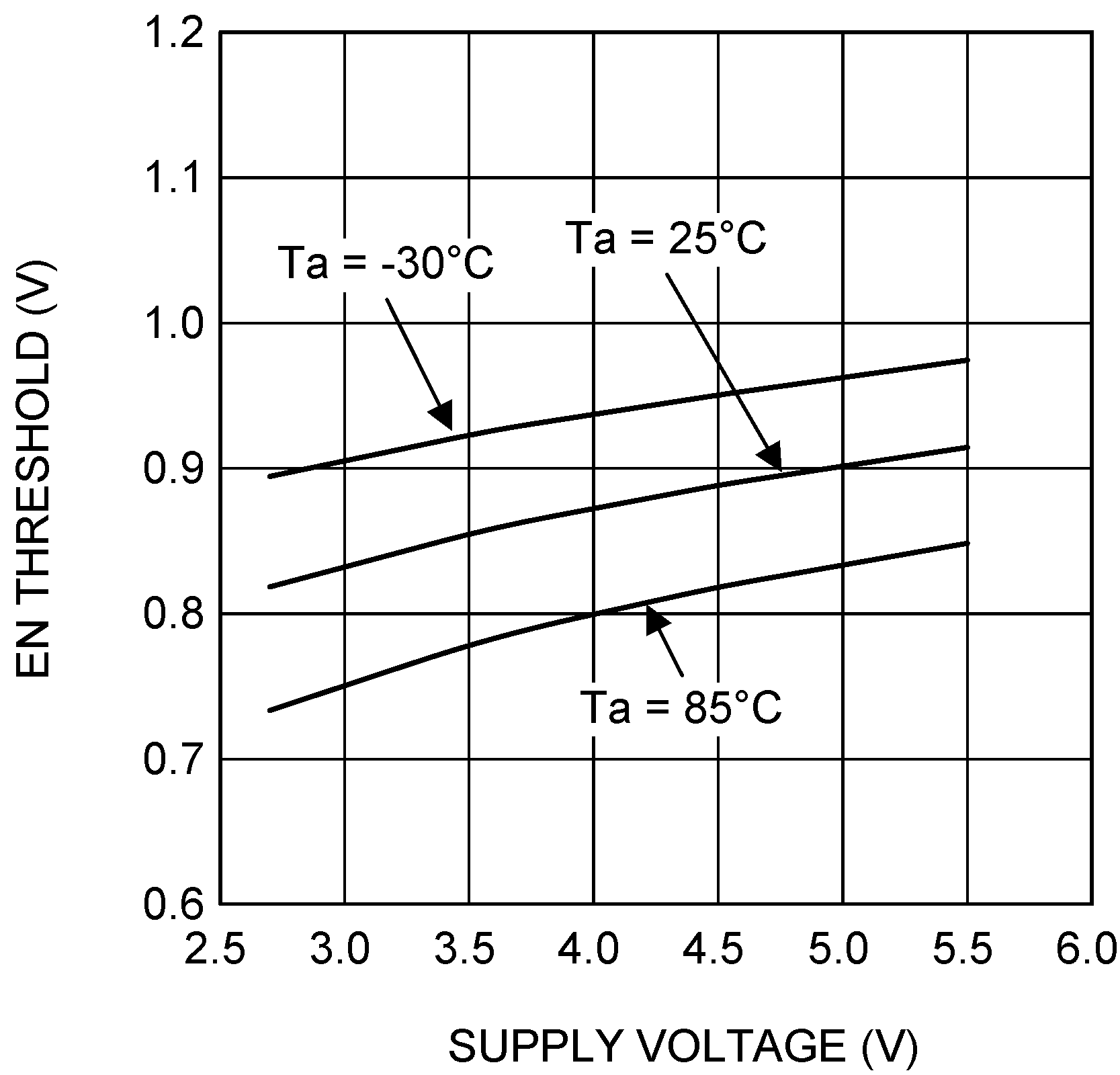
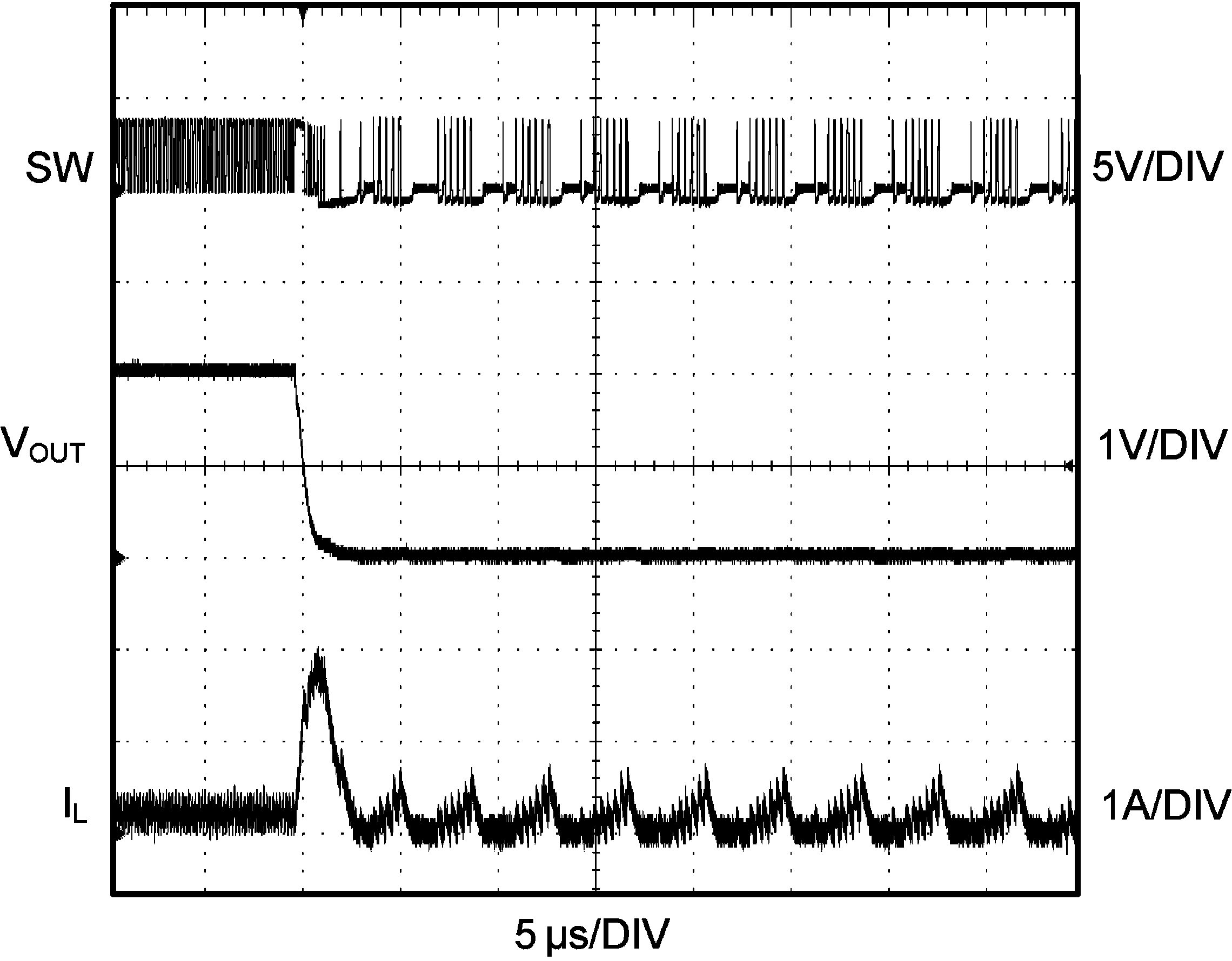
| VOUT = 2 V | RLOAD =10 Ω → 0 Ω | |