ZHCSAP9E October   2011  – August 2015 LM3242

PRODUCTION DATA.  

  1. 特性
  2. 应用
  3. 说明
  4. 修订历史记录
  5. Pin Configuration and Functions
  6. Specifications
    1. 6.1 Absolute Maximum Ratings
    2. 6.2 ESD Ratings
    3. 6.3 Recommended Operating Conditions
    4. 6.4 Thermal Information
    5. 6.5 Electrical Characteristics
    6. 6.6 System Characteristics
    7. 6.7 Timing Requirements
    8. 6.8 Typical Characteristics
  7. Detailed Description
    1. 7.1 Overview
    2. 7.2 Functional Block Diagram
    3. 7.3 Feature Description
      1. 7.3.1 Circuit Operation
      2. 7.3.2 Internal Synchronous Rectification
      3. 7.3.3 Current Limiting
      4. 7.3.4 Dynamically Adjustable Output Voltage
      5. 7.3.5 Thermal Overload Protection
      6. 7.3.6 Soft Start
    4. 7.4 Device Functional Modes
      1. 7.4.1 PWM Mode Operation
      2. 7.4.2 Bypass Mode Operation
      3. 7.4.3 ECO Mode Operation
      4. 7.4.4 Sleep Mode Operation
      5. 7.4.5 Shutdown Mode
  8. Application and Implementation
    1. 8.1 Application Information
      1. 8.1.1 Setting The Output Voltage
      2. 8.1.2 FB
    2. 8.2 Typical Application
      1. 8.2.1 Design Requirements
      2. 8.2.2 Detailed Design Procedure
        1. 8.2.2.1 Inductor Selection
          1. 8.2.2.1.1 Method 1
          2. 8.2.2.1.2 Method 2
        2. 8.2.2.2 Capacitor Selection
      3. 8.2.3 Application Curves
  9. Power Supply Recommendations
  10. 10Layout
    1. 10.1 Layout Guidelines
      1. 10.1.1 PCB Considerations
        1. 10.1.1.1 Energy Efficiency
        2. 10.1.1.2 EMI
      2. 10.1.2 Manufacturing Considerations
      3. 10.1.3 LM3242 Evaluation Board
        1. 10.1.3.1 Component Placement
    2. 10.2 Layout Examples
    3. 10.3 DSBGA Package Assembly and Use
  11. 11器件和文档支持
    1. 11.1 器件支持
      1. 11.1.1 Third-Party Products Disclaimer
    2. 11.2 文档支持
      1. 11.2.1 相关文档 
    3. 11.3 社区资源
    4. 11.4 商标
    5. 11.5 静电放电警告
    6. 11.6 Glossary
  12. 12机械、封装和可订购信息

封装选项

机械数据 (封装 | 引脚)
散热焊盘机械数据 (封装 | 引脚)
订购信息

5 Pin Configuration and Functions

YFQ Package
9-Pin DSBGA
Top View (left); Bottom View (right)
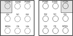
LM3242 30122204.gif

Pin Functions

PIN TYPE DESCRIPTION
NUMBER NAME
A1 VCON A/I Voltage control analog input. VCON controls VOUT in PWM and ECO modes. VCON may also be used to force bypass condition by setting VCON > VIN/2.5.
A2 SGND G Signal ground for analog and control circuitry.
A3 PGND G Power ground for the power MOSFETs and gate drive circuitry
B1 EN D/I Enable Input. Set this digital input high for normal operation. For shutdown, set low. Do not leave EN pin floating.
B2 NC Do not connect to PGND directly — Internally connected to SGND.
B3 SW P/O Switching node connection to the internal PFET switch and NFET synchronous rectifier. Connect to an inductor with a saturation current rating that exceeds the maximum Switch Peak Current Limit specification of the LM3242.
C1 BPEN D/I Bypass Enable input. Set this digital input high to force bypass operation. For normal operation with automatic bypass, set low or connect to ground. Do not leave this pin floating.
C2 FB A Feedback analog input and bypass FET output. Connect to the output at the output filter capacitor.
C3 VIN P/I Voltage supply input for SMPS converter.