ZHCSOW0J January   2000  – March 2022 LM158-N , LM258-N , LM2904-N , LM358-N

PRODUCTION DATA  

  1. 特性
  2. 应用
  3. 说明
  4. Revision History
  5. Pin Configuration and Functions
  6. Specifications
    1. 6.1 Absolute Maximum Ratings
    2. 6.2 ESD Ratings
    3. 6.3 Recommended Operating Conditions
    4. 6.4 Thermal Information
    5. 6.5 Electrical Characteristics: LM158A, LM358A, LM158, LM258
    6. 6.6 Electrical Characteristics: LM358, LM2904
    7. 6.7 Typical Characteristics
  7. Detailed Description
    1. 7.1 Overview
    2. 7.2 Functional Block Diagram
    3. 7.3 Feature Description
    4. 7.4 Device Functional Modes
  8. Application and Implementation
    1. 8.1 Application Information
    2. 8.2 Typical Applications
      1. 8.2.1 Noninverting DC Gain
        1. 8.2.1.1 Design Requirements
        2. 8.2.1.2 Detailed Design Procedure
        3. 8.2.1.3 Application Curve
      2. 8.2.2 System Examples
        1. 8.2.2.1 Typical Single-Supply Applications
  9. Power Supply Recommendations
  10. 10Layout
    1. 10.1 Layout Guidelines
    2. 10.2 Layout Example
  11. 11Device and Documentation Support
    1. 11.1 接收文档更新通知
    2. 11.2 支持资源
    3. 11.3 Trademarks
    4. 11.4 Electrostatic Discharge Caution
    5. 11.5 术语表
  12. 12Mechanical, Packaging, and Orderable Information

封装选项

机械数据 (封装 | 引脚)
散热焊盘机械数据 (封装 | 引脚)
订购信息

Noninverting DC Gain

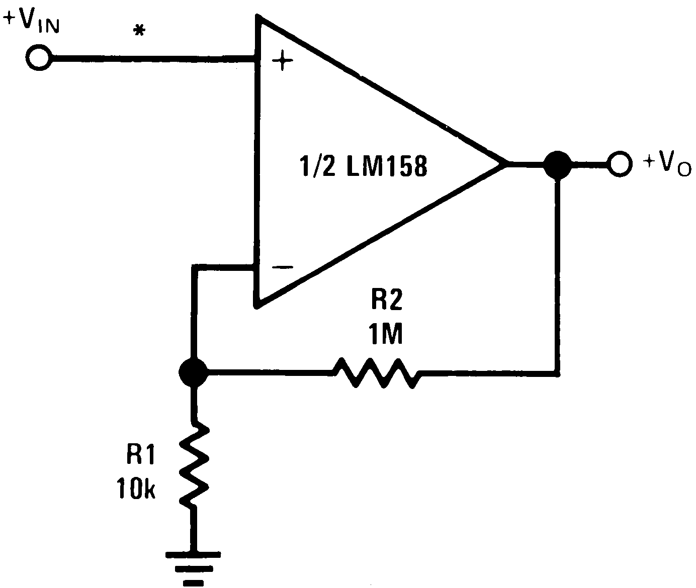
Figure 8-1 shows a high input impedance non-inverting circuit. This circuit gives a closed-loop gain equal to the ratio of the sum of R1 and R2 to R1 and a closed-loop 3 dB bandwidth equal to the amplifier unity-gain frequency divided by the closed-loop gain. This design has the benefit of a very high input impedance, which is equal to the differential input impedance multiplied by loop gain. (Open loop gain/Closed loop gain.) In DC coupled applications, input impedance is not as important as input current and its voltage drop across the source resistance. Note that the amplifier output will go into saturation if the input is allowed to float. This may be important if the amplifier must be switched from source to source.
GUID-7522CACA-35A1-455F-ACE0-4E72B6D90ABF-low.png
*R not needed due to temperature independent IIN
Figure 8-1 Non-Inverting DC Gain (0-V Output)