SNOSD55 June 2017 LF356-MIL
PRODUCTION DATA.
- 1 Features
- 2 Applications
- 3 Description
- 4 Revision History
- 5 Pin Configuration and Functions
-
6 Specifications
- 6.1 Absolute Maximum Ratings
- 6.2 ESD Ratings
- 6.3 Recommended Operating Conditions
- 6.4 Thermal Information
- 6.5 AC Electrical Characteristics, TA = TJ = 25°C, VS = ±15 V
- 6.6 DC Electrical Characteristics, TA = TJ = 25°C, VS = ±15 V
- 6.7 DC Electrical Characteristics
- 6.8 Power Dissipation Ratings
- 6.9 Typical Characteristics
- 7 Detailed Description
- 8 Application and Implementation
- 9 Power Supply Recommendations
- 10Layout
- 11Device and Documentation Support
- 12Mechanical, Packaging, and Orderable Information
10 Layout
10.1 Layout Guidelines
10.1.1 Printed-Circuit-Board Layout For High-Impedance Work
It is generally recognized that any circuit which must operate with less than 1000 pA of leakage current requires special layout of the PCB. When one wishes to take advantage of the low input bias current of the LF356-MIL, typically less than 30 pA, it is essential to have an excellent layout. Fortunately, the techniques of obtaining low leakages are quite simple. First, the user must not ignore the surface leakage of the PCB, even though it may sometimes appear acceptably low, because under conditions of high humidity or dust or contamination, the surface leakage will be appreciable.
To minimize the effect of any surface leakage, lay out a ring of foil completely surrounding the inputs of the LF356-MIL and the terminals of capacitors, diodes, conductors, resistors, relay terminals, and so forth, connected to the inputs of the op amp, as in Figure 39. To have a significant effect, guard rings must be placed on both the top and bottom of the PCB. This PC foil must then be connected to a voltage that is at the same voltage as the amplifier inputs, because no leakage current can flow between two points at the same potential. For example, a PCB trace-to-pad resistance of 10 TΩ, which is normally considered a very large resistance, could leak 5 pA if the trace were a 5-V bus adjacent to the pad of the input. If a guard ring is used and held close to the potential of the amplifier inputs, it will significantly reduce this leakage current.
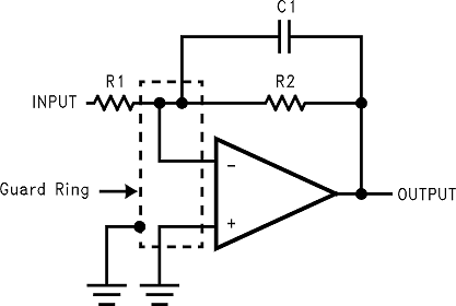 Figure 35. Inverting Amplifier
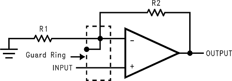 Figure 36. Noninverting Amplifier
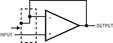 Figure 37. Typical Connections Of Guard Rings
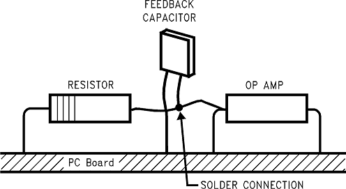
The designer should be aware that when it is inappropriate to lay out a PCB for the sake of just a few circuits, there is another technique which is even better than a guard ring on a PCB: Do not insert the input pin of the amplifier into the board at all, but bend it up in the air and use only air as an insulator. Air is an excellent insulator. In this case you may have to forego some of the advantages of PCB construction, but the advantages are sometimes well worth the effort of using point-to-point up-in-the-air wiring. See Figure 38.
Another potential source of leakage that might be overlooked is the device package. When the LF356-MIL is manufactured, the device is always handled with conductive finger cots. This is to assure that salts and skin oils do not cause leakage paths on the surface of the package. We recommend that these same precautions be adhered to, during all phases of inspection, test and assembly.
10.2 Layout Example
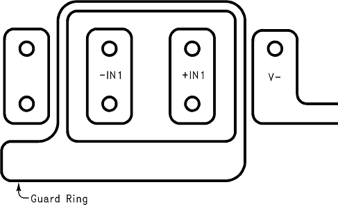 Figure 39. Examples Of Guard
Ring In PCB Layout