ZHCSFW0C July 2016 – December 2016 INA260
PRODUCTION DATA.
- 1 特性
- 2 应用
- 3 说明
- 4 修订历史记录
- 5 Related Products
- 6 Pin Configuration and Functions
- 7 Specifications
-
8 Detailed Description
- 8.1 Overview
- 8.2 Functional Block Diagram
- 8.3 Feature Description
- 8.4 Device Functional Modes
- 8.5 Programming
- 8.6
Register Maps
- 8.6.1 Configuration Register (00h) (Read/Write)
- 8.6.2 Current Register (01h) (Read-Only)
- 8.6.3 Bus Voltage Register (02h) (Read-Only)
- 8.6.4 Power Register (03h) (Read-Only)
- 8.6.5 Mask/Enable Register (06h) (Read/Write)
- 8.6.6 Alert Limit Register (07h) (Read/Write)
- 8.6.7 Manufacturer ID Register (FEh) (Read-Only)
- 8.6.8 Die ID Register (FFh) (Read-Only)
- 9 Application and Implementation
- 10Power Supply Recommendations
- 11Layout
- 12器件和文档支持
- 13机械、封装和可订购信息
11 Layout
11.1 Layout Guidelines
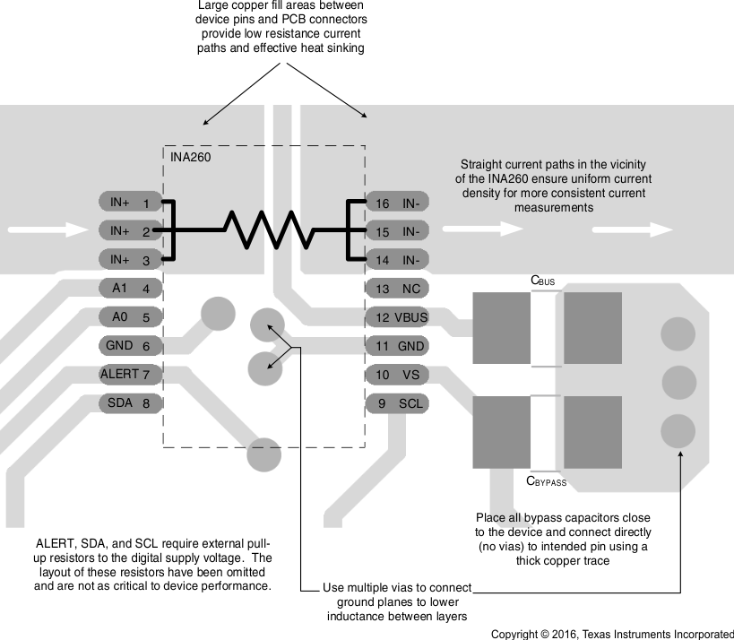
Connections to the internal shunt resistor should be connected directly into and out of the shunt resistor pins to encourage uniform current flow through the device. The trace width should be sized correctly to handle the desired current flow. Place the power-supply bypass capacitor as close as possible to the supply and ground pins. Use of multiple vias to connect the device ground to the bypass capacitor grounds is recommended if there is not direct connection on the top layer.
11.2 Layout Example

1.
Figure 33. INA260 Layout Example
NOTE:
Connect the VBUS pin to the power supply rail.