ZHCSSF8A September 2000 – August 2023 INA141
PRODUCTION DATA
7.1.5 Input Bias Current Return Path
The input impedance of the INA141 is extremely high—approximately 1010 Ω. However, a path must be provided for the input bias current of both inputs. This input bias current is approximately ±2 nA. High input impedance means that this input bias current changes very little with varying input voltage.
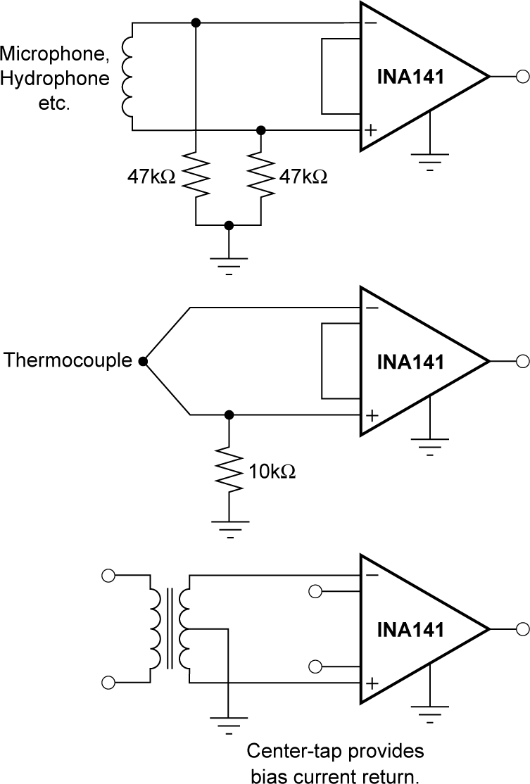
Input circuitry must provide a path for this input bias current for proper operation. Figure 7-3 shows various provisions for an input bias current path. Without a bias current path, the inputs float to a potential that exceeds the common-mode range of the INA141 and the input amplifiers saturate.
If the differential source resistance is low, the bias current return path can be connected to one input (see the thermocouple example in Figure 7-3). With higher source impedance, using two equal resistors provides a balanced input with possible advantages of lower input offset voltage due to bias current and better high-frequency common-mode rejection.
 Figure 7-3 Providing an Input Common-Mode
Current Path.