SBOS508A December 2009 – December 2015 INA129-EP
PRODUCTION DATA.
9 Power Supply Recommendations
The minimum power supply voltage for INA129-EP is ±2.25 V and the maximum power supply voltage is ±18 V. This minimum and maximum range covers a wide range of power supplies; but for optimum performance, ±15 V is recommended. TI recommends adding a bypass capacitor at the input to compensate for the layout and power supply source impedance.
9.1 Low Voltage Operation
The INA129-EP can be operated on power supplies as low as ±2.25 V. Performance remains excellent with power supplies ranging from ±2.25 V to ±18 V. Most parameters vary only slightly throughout this supply voltage range.
Operation at very low supply voltage requires careful attention to assure that the input voltages remain within their linear range. Voltage swing requirements of internal nodes limit the input common-mode range with low power supply voltage. Figure 5 and Figure 6 show the range of linear operation for ±15 V, ±5 V, and ±2.5 V supplies.
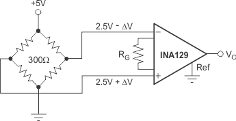 Figure 23. Bridge Amplifier
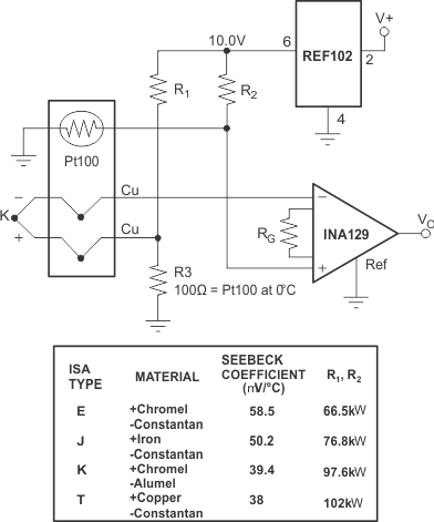 Figure 25. Thermocouple Amplifier With RTD Cold-Junction Compensation
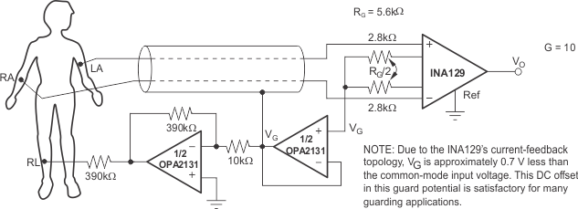 Figure 27. ECG Amplifier With Right-Leg Drive
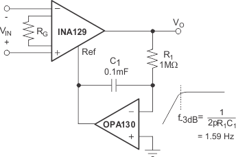 Figure 24. AC-Coupled Instrumentation Amplifier
 Figure 26. Differential Voltage to Current Converter