ZHCSET2A November   2015  – January 2016 HDC1080

PRODUCTION DATA.  

  1. 特性
  2. 应用
  3. 说明
  4. 典型应用
  5. 修订历史记录
  6. Pin Configuration and Functions
  7. Specifications
    1. 7.1 Absolute Maximum Ratings
    2. 7.2 ESD Ratings
    3. 7.3 Recommended Operating Conditions
    4. 7.4 Thermal Information
    5. 7.5 Electrical Characteristics
    6. 7.6 I2C Interface Electrical Characteristics
    7. 7.7 I2C Interface Timing Requirements
    8. 7.8 Typical Characteristics
  8. Detailed Description
    1. 8.1 Overview
    2. 8.2 Functional Block Diagram
    3. 8.3 Feature Description
      1. 8.3.1 Power Consumption
      2. 8.3.2 Voltage Supply Monitoring
      3. 8.3.3 Heater
    4. 8.4 Device Functional Modes
    5. 8.5 Programming
      1. 8.5.1 I2C Interface
        1. 8.5.1.1 Serial Bus Address
        2. 8.5.1.2 Read and Write Operations
        3. 8.5.1.3 Device Measurement Configuration
    6. 8.6 Register Map
      1. 8.6.1 Temperature Register
      2. 8.6.2 Humidity Register
      3. 8.6.3 Configuration Register
      4. 8.6.4 Serial Number Registers
      5. 8.6.5 Manufacturer ID Register
      6. 8.6.6 Device Register ID
  9. Application and Implementation
    1. 9.1 Application Information
    2. 9.2 Typical Application
      1. 9.2.1 Design Requirements
      2. 9.2.2 Detailed Design Procedure
      3. 9.2.3 Application Curve
    3. 9.3 Implementation and Usage Recommendations
      1. 9.3.1 Soldering
      2. 9.3.2 Chemical Exposure and Sensor Protection
      3. 9.3.3 High Temperature and Humidity Exposure
  10. 10Power Supply Recommendations
  11. 11Layout
    1. 11.1 Layout Guidelines
    2. 11.2 Layout Example
  12. 12器件和文档支持
    1. 12.1 文档支持
      1. 12.1.1 相关文档
    2. 12.2 社区资源
    3. 12.3 商标
    4. 12.4 静电放电警告
    5. 12.5 Glossary
  13. 13机械、封装和可订购信息

封装选项

机械数据 (封装 | 引脚)
散热焊盘机械数据 (封装 | 引脚)
订购信息

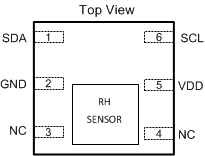
6 Pin Configuration and Functions

DMB Package
6 Pin PWSON
Top View
HDC1080 PINOUT.gif

Pin Functions

PIN I/O TYPE(1) DESCRIPTION
NAME NO.
SDA 1 I/O Serial data line for I2C, open-drain; requires a pull-up resistor to VDD
GND 2 G Ground
NC 3,4 - These pins may be left floating, or connected to GND
VDD 5 P Supply Voltage
SCL 6 I Serial clock line for I2C, open-drain; requires a pull-up resistor to VDD
DAP DAP - Die Attach Pad. Should be left floating. (On bottom of the device, not shown in the figure)
(1) P=Power, G=Ground, I=Input, O=Output