ZHCSEN9A NOVEMBER 2014 – January 2016 DS90UB940-Q1
PRODUCTION DATA.
- 1 特性
- 2 应用
- 3 说明
- 4 应用 图
- 5 修订历史记录
- 6 Pin Configurations and Functions
-
7 Specifications
- 7.1 Absolute Maximum Ratings
- 7.2 ESD Ratings—JEDEC
- 7.3 ESD Ratings—IEC and ISO
- 7.4 Recommended Operating Conditions
- 7.5 Thermal Information
- 7.6 DC Electrical Characteristics
- 7.7 AC Electrical Characteristics
- 7.8 Timing Requirements for the Serial Control Bus
- 7.9 Switching Characteristics
- 7.10 Timing Diagrams and Test Circuits
- 7.11 Power Sequence
- 7.12 Typical Characteristics
-
8 Detailed Description
- 8.1 Overview
- 8.2 Functional Block Diagram
- 8.3
Feature Description
- 8.3.1 High Speed Forward Channel Data Transfer
- 8.3.2 Low Speed Back Channel Data Transfer
- 8.3.3 FPD-Link III Port Register Access
- 8.3.4 Clock and Output Status
- 8.3.5 LVCMOS VDDIO Option
- 8.3.6 Power Down (PDB)
- 8.3.7 Interrupt Pin — Functional Description and Usage (INTB_IN)
- 8.3.8 General-purpose I/O
- 8.3.9 SPI Communication
- 8.3.10 Backward Compatibility
- 8.3.11 Input Equalization
- 8.3.12 I2S Audio Interface
- 8.3.13 Built-In Self Test (BIST)
- 8.3.14 Internal Pattern Generation
- 8.4 Device Functional Modes
- 8.5
Programming
- 8.5.1 Serial Control Bus
- 8.5.2 Multi-Master Arbitration Support
- 8.5.3 I2C Restrictions on Multi-Master Operation
- 8.5.4 Multi-Master Access to Device Registers for Newer FPD-Link III Devices
- 8.5.5 Multi-Master Access to Device Registers for Older FPD-Link III Devices
- 8.5.6 Restrictions on Control Channel Direction for Multi-Master Operation
- 8.6 Register Maps
- 9 Application and Implementation
- 10Power Supply Recommendations
- 11Layout
- 12器件和文档支持
- 13机械、封装和可订购信息
7 Specifications
7.1 Absolute Maximum Ratings
Over operating free-air temperature range (unless otherwise noted)(1) (2)
(1) Stresses beyond those listed under Absolute Maximum Ratings may cause permanent damage to the device. These are stress ratings only, which do not imply functional operation of the device at these or any other conditions beyond those indicated under Recommended Operating Conditions. Exposure to absolute-maximum-rated conditions for extended periods may affect device reliability.
7.2 ESD Ratings—JEDEC
| VALUE | UNIT | |||
|---|---|---|---|---|
| V(ESD) | Electrostatic discharge | Human-body model (HBM), per AEC Q100-002(1) | ±8000 | V |
| Charged-device model (CDM), per AEC Q100-011 | ±1250 | |||
(1) AEC Q100-002 indicates that HBM stressing shall be in accordance with the ANSI/ESDA/JEDEC JS-001 specification.
7.3 ESD Ratings—IEC and ISO
| VALUE | UNIT | ||||
|---|---|---|---|---|---|
| V(ESD) | Electrostatic discharge | RD = 330 Ω, CS = 150 pF | IEC, powered-up only contact discharge (RIN0+, RIN0-, RIN1+, RIN1-) | ±8000 | V |
| IEC, powered-up only air-gap discharge (RIN0+, RIN0-, RIN1+, RIN1-) | ±15000 | ||||
| RD = 330 Ω, CS = 150 and 330 pF | ISO10605 contact discharge (RIN0+, RIN0-, RIN1+, RIN1-) | ±8000 | V | ||
| ISO10605 air-gap discharge (RIN0+, RIN0-, RIN1+, RIN1-) | ±15000 | ||||
| RD = 2 kΩ, CS = 150 and 330 pF | ISO10605 contact discharge (RIN0+, RIN0-, RIN1+, RIN1-) | ±8000 | V | ||
| ISO10605 air-gap discharge (RIN0+, RIN0-, RIN1+, RIN1-) | ±15000 | ||||
7.4 Recommended Operating Conditions
| MIN | NOM | MAX | UNIT | |
|---|---|---|---|---|
| Supply Voltage (VDD33) | 3.0 | 3.3 | 3.6 | V |
| Supply Voltage (VDD18) | 1.71 | 1.8 | 1.89 | V |
| Supply Voltage (VDD12) | 1.14 | 1.2 | 1.26 | V |
| Operating Free Air Temperature (TA) | −40 | 25 | 105 | °C |
| Pixel Clock Frequency (Single Link) | 25 | 96 | MHz | |
| Pixel Clock Frequency (Dual Link) | 50 | 170 | MHz | |
| Supply Noise -- VDD33 (DC-50MHz) | 100 | mVP-P | ||
| Supply Noise -- VDD18 (DC-50MHz) | 50 | mVP-P | ||
| Supply Noise -- VDD12 (DC-50MHz) | 25 | mVP-P |
7.5 Thermal Information
| THERMAL METRIC(1) | DS90UB940-Q1 | UNIT | |
|---|---|---|---|
| WQFN (NKD) | |||
| 64 PINS | |||
| RθJA | Junction-to-ambient thermal resistance | 24.8 | °C/W |
| RθJC(top) | Junction-to-case (top) thermal resistance | 6.2 | |
| RθJB | Junction-to-board thermal resistance | 3.6 | |
| ψJT | Junction-to-top characterization parameter | 0.1 | |
| ψJB | Junction-to-board characterization parameter | 3.6 | |
| RθJC(bot) | Junction-to-case (bottom) thermal resistance | 0.6 | |
(1) For more information about traditional and new thermal metrics, see the IC Package Thermal Metrics application report, SPRA953.
7.6 DC Electrical Characteristics
Over recommended operating supply and temperature ranges unless otherwise specified.| PARAMETER | TEST CONDITIONS | PIN/FREQ. | MIN | TYP | MAX | UNIT | |
|---|---|---|---|---|---|---|---|
| 3.3V LVCMOS I/O (VDDIO = 3.3V ± 10%) | |||||||
| VIH | High Level Input Voltage | PDB, BISTEN, BISTC, GPIO[3:0], D_GPIO[3:0], I2S_DA, I2S_DB, I2S_DC, I2S_DD, I2S_CLK, I2S_WC, LOCK, PASS | 2.0 | VDDIO | V | ||
| VIL | Low Level Input Voltage | 0 | 0.8 | V | |||
| IIN | Input Current | VIN = 0V or VDDIO | -10 | 10 | µA | ||
| VOH | High Level Output Voltage | IOH = -4mA | 2.4 | VDDIO | V | ||
| VOL | Low Level Output Voltage | IOL = +4mA | 0 | 0.4 | V | ||
| IOS | Output Short Circuit Current | VOUT = 0V | -55 | mA | |||
| IOZ | Tri-state Output Current | PDB = 0V VOUT = 0V or VDDIO |
-20 | 20 | µA | ||
| CIN | Input Capacitance | 10 | pF | ||||
| 1.8V LVCMOS I/O (VDDIO = 1.8V ± 5%) | |||||||
| VIH | High Level Input Voltage | PDB, BISTEN, BISTC, GPIO[3:0], D_GPIO[3:0], I2S_DA, I2S_DB, I2S_DC, I2S_DD, I2S_CLK, I2S_WC, LOCK, PASS | 0.65 * VDDIO | VDDIO | V | ||
| VIL | Low Level Input Voltage | 0 | 0.35 * VDDIO | V | |||
| IIN | Input Current | VIN = 0V or VDDIO | -10 | 10 | µA | ||
| VOH | High Level Output Voltage | IOH = -4mA | VDDIO-0.45 | VDDIO | V | ||
| VOL | Low Level Output Voltage | IOL = +4mA | 0 | 0.45 | V | ||
| IOS | Output Short Circuit Current | VOUT = 0V | -35 | mA | |||
| IOZ | Tri-state Output Current | PDB = 0V VOUT = 0V or VDDIO |
-20 | 20 | µA | ||
| CIN | Input Capacitance | 10 | pF | ||||
| SERIAL CONTROL BUS (VDDIO = 1.8V ± 5% OR 3.3V ± 10%) | |||||||
| VIH | Input High Level | I2C_SDA, I2C_SCL | 0.7 * VDDIO | VDD33 | V | ||
| VIL | Input Low Level | GND | 0.3 * VDDIO | V | |||
| VHY | Input Hysteresis | >50 | mV | ||||
| VOL | Output Low Level | IOL = +4mA | 0 | 0.4 | V | ||
| IIN | Input Current | VIN = 0V or VDDIO | -10 | 10 | µA | ||
| FPD-LINK III CML INPUT | |||||||
| VTH | Differential Threshold High Voltage | VCM = 2.1V (Internal VBIAS) | RIN0+, RIN0- RIN1+, RIN1- |
50 | mV | ||
| VTL | Differential Threshold Low Voltage | -50 | mV | ||||
| VID | Input Differential Threshold | 100 | mV | ||||
| VCM | Differential Common-mode Voltage | 2.1 | V | ||||
| RT | Internal Termination Resistor - Differential | 80 | 100 | 120 | Ω | ||
| HSTX DRIVER | |||||||
| VCMTX | HS transmit static common-mode voltage | CSI0_D3±, CSI0_D2±, CSI0_D1±, CSI0_D0±, CSI0_CLK±, CSI1_D3±, CSI1_D2±, CSI1_D1±, CSI1_D0±, CSI1_CLK± | 150 | 200 | 250 | mV | |
| |ΔVCMTX(1,0)| | VCMTX mismatch when output is 1 or 0 | 5 | mVP-P | ||||
| |VOD| | HS transmit differential voltage | 140 | 200 | 270 | mV | ||
| |ΔVOD| | VOD mismatch when output is 1 or 0 | 14 | mV | ||||
| VOHHS | HS output high voltage | 360 | mV | ||||
| ZOS | Single-ended output impedance | 40 | 50 | 62.5 | Ω | ||
| ΔZOS | Mismatch in single-ended output impedance | 10 | % | ||||
| LPTX DRIVER | |||||||
| VOH | High Level Output Voltage | IOH = -4mA | CSI0_D3±, CSI0_D2±, CSI0_D1±, CSI0_D0±, CSI0_CLK±, CSI1_D3±, CSI1_D2±, CSI1_D1±, CSI1_D0±, CSI1_CLK± | 1.05 | 1.2 | 1.3 | V |
| VOL | Low Level Output Voltage | IOL = +4mA | -50 | 50 | mV | ||
| ZOLP | Output impedance | 110 | Ω | ||||
| LOOP-THROUGH MONITOR OUTPUT | |||||||
| VODp-p | Differential Output Voltage | RL = 100Ω | CMLOUTP, CMLOUTN | 360 | mV | ||
| SUPPLY CURRENT | |||||||
| PT | Total Power Consumption, Normal Operation | Checkerboard Pattern, 170MHz. See Figure 1. 2-lane FPD-Link III Input, 2 MIPI lanes Output |
VDD | 628 | 875 | mW | |
| PZ | Total Power Consumption, Power-Down Mode | PDB = 0V | 10 | 45 | mW | ||
| IDD12 | Supply Current, Normal Operation | Checkerboard Pattern, 96MHz. See Figure 1. 1-lane FPD-Link III Input, 2 MIPI lanes Output |
VDD12 = 1.2 V | 150 | 250 | mA | |
| IDD33 | VDD33 = 3.6 V | 90 | 122 | mA | |||
| IDDIO | VDDIO = 1.89 V | 1 | 6 | mA | |||
| VDDIO = 3.6 V | 1 | 6 | mA | ||||
| IDD12 | Supply Current, Normal Operation | Checkerboard Pattern, 96MHz. See Figure 1. 1-lane FPD-Link III Input, 4 MIPI lanes Output |
VDD12 = 1.2 V | 125 | 225 | mA | |
| IDD33 | VDD33 = 3.6 V | 90 | 122 | mA | |||
| IDDIO | VDDIO = 1.89 V | 1 | 6 | mA | |||
| VDDIO = 3.6 V | 1 | 6 | mA | ||||
| IDD12 | Supply Current, Normal Operation | Checkerboard Pattern, 170MHz. See Figure 1. 2-lane FPD-Link III Input, 2 MIPI lanes Output |
VDD12 = 1.2 V | 250 | 345 | mA | |
| IDD33 | VDD33 = 3.6 V | 90 | 122 | mA | |||
| IDDIO | VDDIO = 1.89 V | 1 | 6 | mA | |||
| VDDIO = 3.6 V | 1 | 6 | mA | ||||
| IDD12 | Supply Current, Normal Operation | Checkerboard Pattern, 170MHz. See Figure 1. 2-lane FPD-Link III Input, 4 MIPI lanes Output |
VDD12 = 1.2 V | 220 | 300 | mA | |
| IDD33 | VDD33 = 3.6 V | 90 | 122 | mA | |||
| IDDIO | VDDIO = 1.89 V | 1 | 6 | mA | |||
| VDDIO = 3.6 V | 1 | 6 | mA | ||||
| IDD12Z | Supply Current, Power Down Mode | PDB = 0 V | VDD12 = 1.2 V | 2 | 30 | mA | |
| IDD33Z | VDD33 = 3.6 V | 2 | 8 | mA | |||
| IDDIOZ | VDDIO = 1.89 V | 0.1 | 0.3 | mA | |||
| VDDIO = 3.6 V | 0.1 | 0.3 | mA | ||||
(1) Parameter is specified by bench characterization and is not tested in production.
7.7 AC Electrical Characteristics
Over recommended operating supply and temperature ranges unless otherwise specified.| PARAMETER | TEST CONDITIONS | PIN/FREQ. | MIN | TYP | MAX | UNIT | |
|---|---|---|---|---|---|---|---|
| GPIO BIT RATE | |||||||
| Rb,FC | Forward Channel Bit Rate | PCLK = 25MHz - 170MHz(3) | GPIO[3:0] | 0.25 * PCLK | Mbps | ||
| Rb,BC | Back Channel Bit Rate | 133 | kbps | ||||
| Rb,BC | Back Channel Bit Rate | High Speed (2-lane Mode), 1 D_GPIO active. See Table 4. |
D_GPIO[3:0] | 2.0 | Mbps | ||
| High Speed (2-lane Mode), 2 D_GPIO's active. See Table 4. |
1.33 | Mbps | |||||
| High Speed (2-lane Mode), 4 D_GPIO's active. See Table 4. |
800 | kbps | |||||
| Normal mode. See Table 4. | 133 | kbps | |||||
| tGPIO,FC | GPIO Pulse Width, Forward Channel | GPIO[3:0] | >2 / PCLK(3) | s | |||
| tGPIO,BC | GPIO Pulse Width, Back Channel | GPIO[3:0] | 20 | μs | |||
| RESET | |||||||
| tLRST | PDB Reset Low Pulse | PDB | 2 | ms | |||
| LOOP-THROUGH MONITOR OUTPUT | |||||||
| EW | Differential Output Eye Opening Width | RL = 100Ω, Jitter frequency > PCLK(3) / 40 See Figure 2. |
CMLOUTP, CMLOUTN | 0.4 | UI | ||
| EH | Differential Output Eye Height | >300 | mV | ||||
| FPD-LINK III CML INPUT | |||||||
| tDDLT | Lock Time | See Figure 4. | RIN0+, RIN0-, RIN1+, RIN1- |
5 | 10(1) | ms | |
| I2S TRANSMITTER | |||||||
| tJ,I2S | Clock Output Jitter | I2S_CLK | 2 | ns | |||
| tI2S | I2S Clock Period(2) | See Figure 9. | >2 / PCLK(3) or >77 | ns | |||
| tHC,I2S | I2S Clock High Time(2) | See Figure 9. | 0.48 | tI2S | |||
| tLC,I2S | I2S Clock Low Time(2) | See Figure 9. | 0.48 | tI2S | |||
| tSR,I2S | I2S Set-up Time | See Figure 9. | I2S_DA, I2S_DB, I2S_DC, I2S_DD | 0.4 | tI2S | ||
| tHR,I2S | I2S Hold Time | See Figure 9. | 0.4 | tI2S | |||
(1) This parameter is specified by characterization and is not tested in production.
(2) I2S specifications for tLC,I2S and tHC,I2S pulses must each be greater than 1 PCLK period to ensure sampling and supersedes the 0.35*tI2S requirement. tLC,I2S and tHC,I2S must be longer than the greater of either 0.35*tI2S or 2 * PCLK.
(3) PCLK refers to the equivalent pixel clock frequency, which is equal to the FPD-Link III line rate / 35.
7.8 Timing Requirements for the Serial Control Bus
Over I2C supply and temperature ranges unless otherwise specified.| PARAMETER | TEST CONDITIONS | MIN | TYP | MAX | UNIT | |
|---|---|---|---|---|---|---|
| fSCL | SCL Clock Frequency | Standard Mode | >0 | 100 | kHz | |
| Fast Mode | >0 | 400 | kHz | |||
| Fast Plus Mode | >0 | 1 | MHz | |||
| tLOW | SCL Low Period | Standard Mode | 4.7 | µs | ||
| Fast Mode | 1.3 | µs | ||||
| Fast Plus Mode | 0.5 | µs | ||||
| tHIGH | SCL High Period | Standard Mode | 4.0 | µs | ||
| Fast Mode | 0.6 | µs | ||||
| Fast Plus Mode | 0.26 | µs | ||||
| tHD;STA | Hold time for a start or a repeated start condition Figure 8 |
Standard Mode | 4.0 | µs | ||
| Fast Mode | 0.6 | µs | ||||
| Fast Plus Mode | 0.26 | µs | ||||
| tSU;STA | Set Up time for a start or a repeated start condition Figure 8 |
Standard Mode | 4.7 | µs | ||
| Fast Mode | 0.6 | µs | ||||
| Fast Plus Mode | 0.26 | µs | ||||
| tHD;DAT | Data Hold Time Figure 8 |
Standard Mode | 0 | µs | ||
| Fast Mode | 0 | µs | ||||
| Fast Plus Mode | 0 | µs | ||||
| tSU;DAT | Data Set Up Time Figure 8 |
Standard Mode | 250 | ns | ||
| Fast Mode | 100 | ns | ||||
| Fast Plus Mode | 50 | ns | ||||
| tSU;STO | Set Up Time for STOP Condition Figure 8 |
Standard Mode | 4.0 | µs | ||
| Fast Mode | 0.6 | µs | ||||
| Fast Plus Mode | 0.26 | µs | ||||
| tBUF | Bus Free Time Between STOP and START Figure 8 |
Standard Mode | 4.7 | µs | ||
| Fast Mode | 1.3 | µs | ||||
| Fast Plus Mode | 0.5 | µs | ||||
| tr | SCL & SDA Rise Time, Figure 8 |
Standard Mode | 1000(1) | ns | ||
| Fast Mode | 300(1) | ns | ||||
| Fast Plus Mode | 120(1) | ns | ||||
| tf | SCL & SDA Fall Time, Figure 8 |
Standard Mode | 300(1) | ns | ||
| Fast mode | 300(1) | ns | ||||
| Fast Plus Mode | 120(1) | ns | ||||
| Cb | Capacitive Load for Each Bus Line | Standard Mode | 400 | pF | ||
| Fast Mode | 400 | pF | ||||
| Fast Plus Mode | 550 | pF | ||||
| tSP | Input Filter | Fast Mode | 50 | ns | ||
| Fast Plus Mode | 50 | ns |
7.9 Switching Characteristics
Over recommended operating supply and temperature ranges unless otherwise specified.| PARAMETER | TEST CONDITIONS | PIN/FREQ. | MIN | TYP | MAX | UNIT | |
|---|---|---|---|---|---|---|---|
| HSTX DRIVER | |||||||
| HSTXDBR | Data bit rate(1) | MIPI 2 Lanes | CSI0_D0± CSI0_D1± CSI0_D2± CSI0_D3± CSI1_D0± CSI1_D1± CSI1_D2± CSI1_D3± CSI0_CLK± CSI1_CLK± |
350 | 1344 | Mbps | |
| MIPI 4 Lanes | 175 | 1190 | |||||
| fCLK | DDR Clock frequency(1) | MIPI 2 Lanes | 175 | 672 | MHz | ||
| MIPI 4 Lanes | 87.5 | 595 | |||||
| ΔVCMTX(HF) | Common mode voltage variations HF(1) | Above 450MHz | 15 | mVRMS | |||
| ΔVCMTX(LF) | Common mode voltage variations LF(1) | Between 50 and 450MHz | 25 | mVRMS | |||
| tRHS
tFHS |
20% to 80% Rise and Fall HS(1) | HS bit rates ≤ 1 Gbps (UI ≥ 1 ns) | 0.3 | UI | |||
| HS bit rates > 1 Gbps (UI < 1 ns) | 0.35 | UI | |||||
| Applicable for all HS bit rates. However, to avoid excessive radiation, bit rates ≤ 1 Gbps (UI ≥ 1 ns), should not use values below 150 ps | 100 | ps | |||||
| SDDTX | TX differential return loss(1) | fLPMAX | -18 | dB | |||
| fH | |||||||
| fMAX | -9 | dB | |||||
| LPTX DRIVER | |||||||
| tRLP | Rise Time LP(1) (3) | 15% to 85% rise time | CSI0_D0± CSI0_D1± CSI0_D2± CSI0_D3± CSI1_D0± CSI1_D1± CSI1_D2± CSI1_D3± CSI0_CLK± CSI1_CLK± |
25 | ns | ||
| tFLP | Fall Time LP(1) (3) | 15% to 85% fall time | 25 | ns | |||
| tREOT | Rise Time Post-EoT(1) (3) | 30%-85% rise time | 35 | ns | |||
| tLP-PULSE-TX | Pulse width of the LP exclusive-OR clock(1) (3) | First LP exclusive-OR clock pulse after Stop state or last pulse before Stop state | 40 | ns | |||
| All other pulses | 20 | ns | |||||
| tLP-PER-TX | Period of the LP exclusive-OR clock(1) | 90 | ns | ||||
| DV/DtSR | Slew rate(1) (3) | Cload = 0pF | 500 | mV/ns | |||
| Cload = 5pF | 300 | mV/ns | |||||
| Cload = 20pF | 250 | mV/ns | |||||
| Cload = 70pF | 150 | mV/ns | |||||
| Cload = 0 to 70pF (Falling Edge Only) | 30 | mV/ns | |||||
| Cload = 0 to 70pF (Rising Edge Only) | 30 | mV/ns | |||||
| Cload = 0 to 70pF (Rising Edge Only) | 30 - 0.075*(VO,INST - 700) | mV/ns | |||||
| CLOAD | Load capacitance(3) | 0 | 70 | pF | |||
| DATA-CLOCK TIMING SPECIFICATIONS (1) (Figure 10) | |||||||
| UIINST | UI instantaneous | fCLK = CSI-2 DDR Clock frequency | CSI0_D0± CSI0_D1± CSI0_D2± CSI0_D3± CSI1_D0± CSI1_D1± CSI1_D2± CSI1_D3± CSI0_CLK± CSI1_CLK± |
1/(fCLK * 2) | UI | ||
| ΔUI | UI variation PCLK = 25 - 96MHz |
UI ≥ 1ns | -10% | 10% | UI | ||
| UI < 1ns | -5% | 5% | UI | ||||
| tSKEW(TX) | Data to Clock Skew (measured at transmitter) Skew between clock and data from ideal center |
Data rate ≤ 1 Gbps | -0.15 | 0.15 | UIINST | ||
| Data rate > 1 Gbps | -0.2 | 0.2 | UIINST | ||||
| CSI-2 TIMING SPECIFICATIONS (1) (Figure 11, Figure 12) | |||||||
| tCLK-MISS | Timeout for receiver to detect absence of Clock transitions and disable the Clock Lane HS-RX | CSI0_D0± CSI0_D1± CSI0_D2± CSI0_D3± CSI1_D0± CSI1_D1± CSI1_D2± CSI1_D3± CSI0_CLK± CSI1_CLK± |
60 | ns | |||
| tCLK-POST | HS exit | 60 + 52*UI | ns | ||||
| tCLK-PRE | Time HS clock shall be driver prior to any associated Data Lane beginning the transition from LP to HS mode | 8 | UI | ||||
| tCLK-PREPARE | Clock Lane HS Entry | 38 | 95 | ns | |||
| tCLK-SETTLE | Time interval during which the HS receiver shall ignore any Clock Lane HS transitions | 95 | 300 | ns | |||
| tCLK-TERM-EN | Time-out at Clock Lane Display Module to enable HS Termination | Time for Dn to reach VTERM-EN | 38 | ns | |||
| tCLK-TRAIL | Time that the transmitter drives the HS-0 state after the last payload clock bit of a HS transmission burst | 60 | ns | ||||
| tCLK-PREPARE + tCLK-ZERO | TCLK-PREPARE + time that the transmitter drives the HS-0 state prior to starting the Clock | 300 | ns | ||||
| tD-TERM-EN | Time for the Data Lane receiver to enable the HS line termination | Time for Dn to reach V-TERM-EN | 35 + 4*UI | ns | |||
| tEOT | Transmitted time interval from the start of tHS-TRAIL to the start of the LP-11 state following a HS burst | see(2) | 105 + 12*UI | ns | |||
| tHS-EXIT | Time that the transmitter drives LP=11 following a HS burst | 100 | ns | ||||
| tHS-PREPARE | Data Lane HS Entry | 40 + 4*UI | 85 + 6*UI | ns | |||
| tHS-PREPARE + tHS-ZERO | tHS-PREPARE + time that the transmitter drives the HS-0 state prior to transmitting the Sync sequence | 145 + 10*UI | ns | ||||
| tHS-SETTLE | Time interval during which the HS receiver shall ignore any Data Lane HS transitions, starting from the beginning of tHS-SETTLE | 85 + 6*UI | 145 + 10*UI | ns | |||
| tHS-SKIP | Time interval during which the HS-RX should ignore any transitions on the Data Lane, following a HS burst. The end point of the interval is defined as the beginning of the LP-11 state following the HS burst. | 40 | 55 + 4*UI | ns | |||
| tHS-TRAIL | Data Lane HS Exit | 60 + 4*UI | ns | ||||
| tLPX | Transmitted length of LP state | 50 | ns | ||||
| tWAKEUP | Recovery Time from Ultra Low Power State (ULPS) | 1 | ms | ||||
(1) Specification is ensured by design and is not tested in production.
(2)
- 1280x720p60; PCLK = 74.25MHz; 4 MIPI lanes reg0x6c=0x02; reg0x6d=0x84
- 1280x720p60; PCLK = 74.25MHz; 2 MIPI lanes reg0x6c=0x02; reg0x6d=0x89
- 640x480p60; PCLK = 25MHz; 4 MIPI lanes reg0x6c=0x02; reg0x6d=0x82
- 640x480p60; PCLK = 25MHz; 2 MIPI lanes reg0x6c=0x02; reg0x6d=0x83
- Other video formats may require additional register configuration.
(3) CLOAD includes the low-frequency equivalent transmission line capacitance. The capacitance of TX and RX are assumed to always be <10 pF. The distributed line capacitance can be up to 50 pF for a transmission line with 2ns delay.
7.10 Timing Diagrams and Test Circuits
 Figure 1. Checkerboard Data Pattern
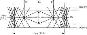 Figure 2. CML Output Driver
 Figure 3. LVCMOS Transition Times
 Figure 4. CML PLL Lock Time
 Figure 5. FPD-Link III Receiver DC VTH/VTL Definition
 Figure 6. Output Data Valid (Setup and Hold) Times
 Figure 7. BIST PASS Waveform
 Figure 8. Serial Control Bus Timing Diagram
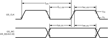 Figure 9. I2S Timing
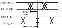 Figure 10. Clock and Data Timing in HS Transmission
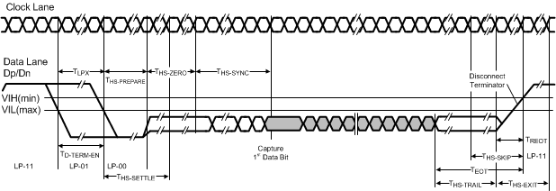 Figure 11. High Speed Data Transmission Burst
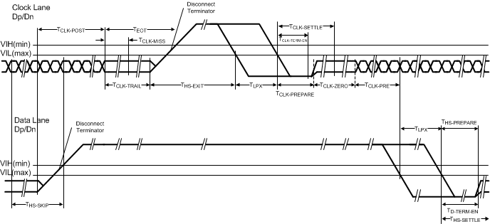 Figure 12. Switching the Clock Lane between Clock Transmission and Low-Power Mode
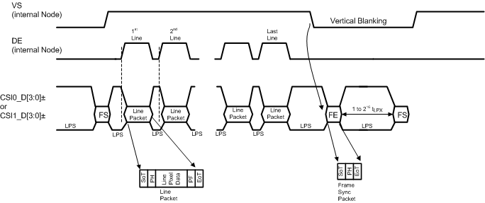 Figure 13. Long Line Packets and Short Frame Sync Packets
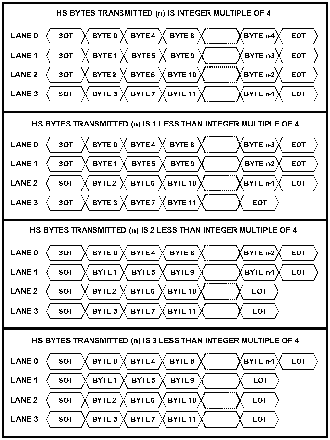 Figure 14. 4 MIPI Data Lane Configuration
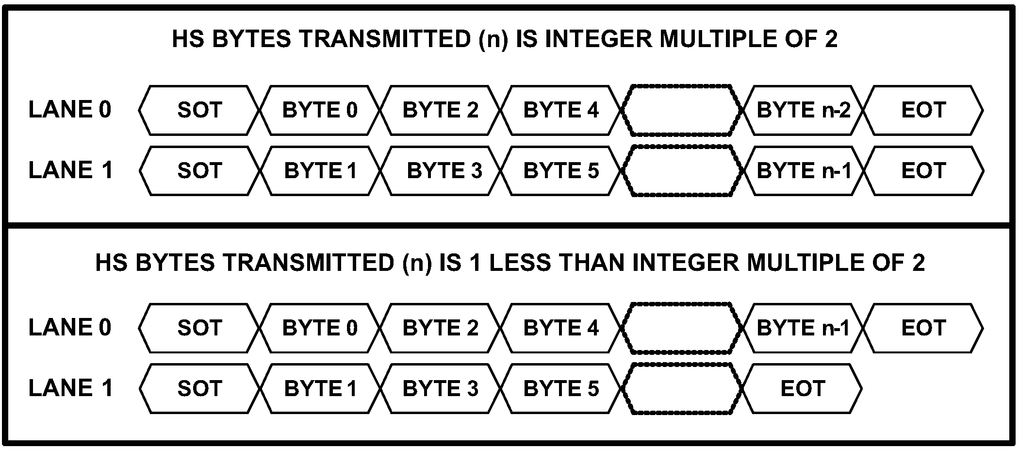 Figure 15. 2 MIPI Data Lane Configuration
7.11 Power Sequence
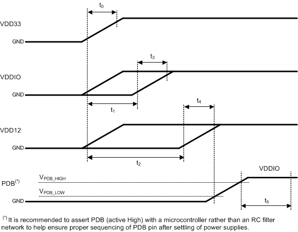 Figure 16. Power Sequence
Table 1. Power-Up Sequencing Constraints
| Symbol | Description | Test Conditions | Min | Typ | Max | Units |
|---|---|---|---|---|---|---|
| VDDIO | VDDIO voltage range | 3.0 | 3.6 | V | ||
| 1.71 | 1.89 | V | ||||
| VDD33 | VDD33 voltage range | 3.0 | 3.6 | V | ||
| VDD12 | VDD12 voltage range | 1.14 | 1.26 | V | ||
| VPDB_LOW | PDB LOW threshold Note: VPDB should not exceed limit for respective I/O voltage before 90% voltage of VDD12 |
VDDIO = 3.3V ± 10% | 0.8 | V | ||
| VDDIO = 1.8V ± 5% | 0.35 * VDDIO | |||||
| VPDB_HIGH | PDB HIGH threshold | VDDIO = 3.3V ± 10% | 2.0 | V | ||
| VDDIO = 1.8V ± 5% | 0.65 * VDDIO | |||||
| t0 | VDD33 rise time | These time constants are specified for rise time of power supply voltage ramp (10% - 90%) | <1.5 | ms | ||
| t3 | VDDIO rise time | These time constants are specified for rise time of power supply voltage ramp (10% - 90%) | <1.5 | ms | ||
| t4 | VDD12 rise time | These time constants are specified for rise time of power supply voltage ramp (10% - 90%) | <1.5 | ms | ||
| t1 | VDDIO delay time | VIL of rising edge (VDDIO ) to VIL of rising edge (VDD_N) The power supplies may be ramped simultaneously. If sequenced, VDD33 should be first, either by itself or with VDDIO (1.8V or 3.3V) or VDD12, with the other rail(s) following in any order. |
>0 | ms | ||
| t2 | VDD12 delay time | |||||
| t5 | Startup time | The part is powered up after the startup time has elapsed from the moment PDB goes HIGH. Local I2C is available to read/write 948/940 registers after this time. | <1 | ms |
7.12 Typical Characteristics
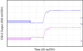 Figure 17. CSI-2 D0± End of Transmission
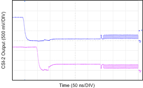 Figure 18. CSI-2 D0± Start of Transmission