SNLS011D July   1999  – August 2016 DS90LV032A

PRODUCTION DATA.  

  1. Features
  2. Applications
  3. Description
  4. Revision History
  5. Pin Configuration and Functions
  6. Specifications
    1. 6.1 Absolute Maximum Ratings
    2. 6.2 ESD Ratings
    3. 6.3 Recommended Operating Conditions
    4. 6.4 Thermal Information
    5. 6.5 Electrical Characteristics
    6. 6.6 Switching Characteristics
    7. 6.7 Dissipation Ratings
    8. 6.8 Typical Characteristics
  7. Parameter Measurement Information
  8. Detailed Description
    1. 8.1 Overview
    2. 8.2 Functional Block Diagram
    3. 8.3 Feature Description
      1. 8.3.1 Fail-Safe Feature
    4. 8.4 Device Functional Modes
  9. Application and Implementation
    1. 9.1 Application Information
      1. 9.1.1 Probing LVDS Transmission Lines
      2. 9.1.2 Cables and Connectors, General Comments
    2. 9.2 Typical Application
      1. 9.2.1 Design Requirements
      2. 9.2.2 Detailed Design Procedure
        1. 9.2.2.1 Probing LVDS Transmission Lines
      3. 9.2.3 Application Curves
  10. 10Power Supply Recommendations
  11. 11Layout
    1. 11.1 Layout Guidelines
      1. 11.1.1 Power Decoupling Recommendations
      2. 11.1.2 Differential Traces
      3. 11.1.3 Termination
    2. 11.2 Layout Example
  12. 12Device and Documentation Support
    1. 12.1 Documentation Support
      1. 12.1.1 Related Documentation
    2. 12.2 Receiving Notification of Documentation Updates
    3. 12.3 Community Resources
    4. 12.4 Trademarks
    5. 12.5 Electrostatic Discharge Caution
    6. 12.6 Glossary
  13. 13Mechanical, Packaging, and Orderable Information

封装选项

机械数据 (封装 | 引脚)
散热焊盘机械数据 (封装 | 引脚)
订购信息

7 Parameter Measurement Information

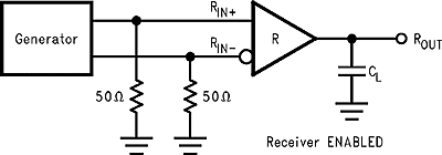
DS90LV032A 10006703.gif Figure 4. Receiver Propagation Delay and Transition Time Test Circuit
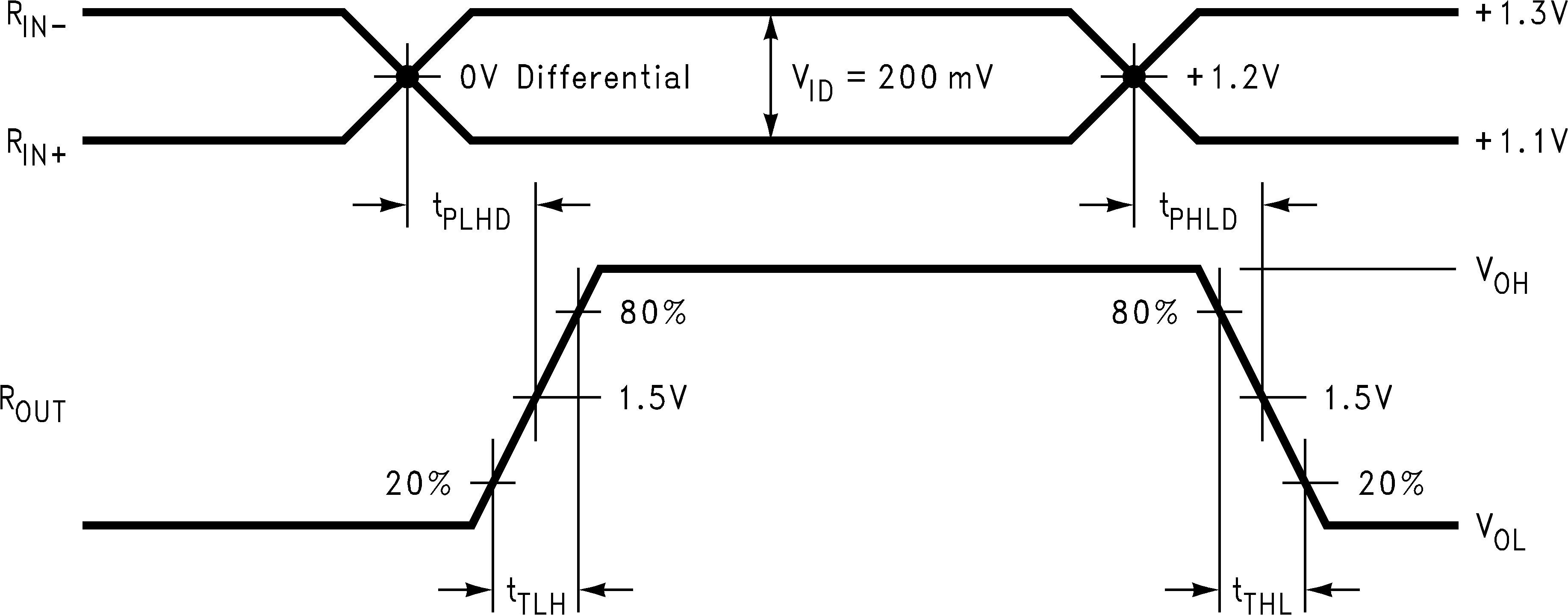
DS90LV032A 10006704.png Figure 5. Receiver Propagation Delay and Transition Time Waveforms
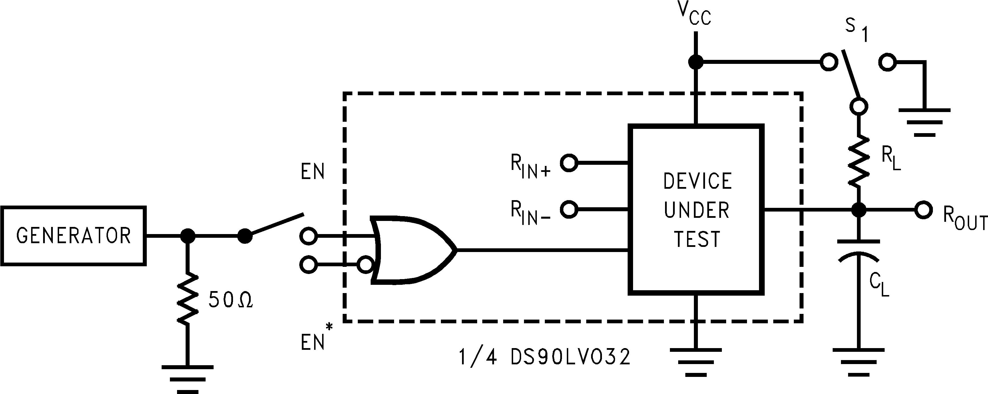
DS90LV032A 10006705.png
CL includes load and test jig capacitance.
S1 = VCC for tPZL, and tPLZ measurements.

S1 = GND for tPZH and tPHZ measurements.
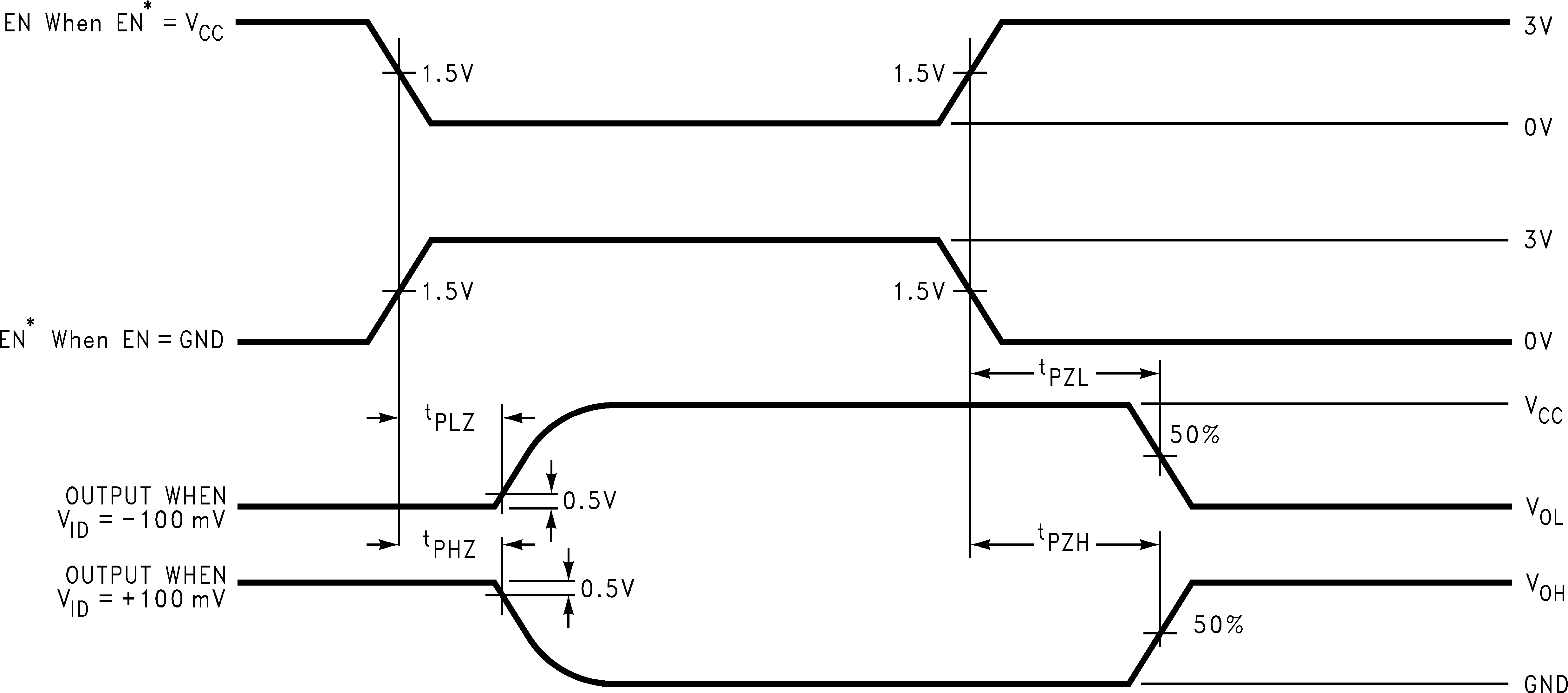
Figure 6. Receiver TRI-STATE Delay Test Circuit
DS90LV032A 10006706.png Figure 7. Receiver TRI-STATE Delay Waveforms