SNLS013F June 1998 – June 2016 DS90LV028A
PRODUCTION DATA.
- 1 Features
- 2 Applications
- 3 Description
- 4 Revision History
- 5 Pin Configuration and Functions
- 6 Specifications
- 7 Parameter Measurement Information
- 8 Detailed Description
- 9 Application and Implementation
- 10Power Supply Recommendations
- 11Layout
- 12Device and Documentation Support
- 13Mechanical, Packaging, and Orderable Information
6 Specifications
6.1 Absolute Maximum Ratings
over operating free-air temperature range (unless otherwise noted)(1)| MIN | MAX | UNIT | ||
|---|---|---|---|---|
| Supply voltage, VCC | –0.3 | 4 | V | |
| Input voltage, RIN+, RIN− | –0.3 | 3.9 | V | |
| Output voltage, ROUT | –0.3 | VCC + 0.3 | V | |
| Maximum package power dissipation at 25°C | D package | 1025 | mW | |
| Derate D package | 8.2 mW/°C above 25°C |
°C | ||
| NGN package | 3.3 | W | ||
| Derate NGN package | 25.6 mW/°C above 25°C |
°C | ||
| Lead temperature range, soldering (4 s) | 260 | °C | ||
| Junction temperature, TJ | 150 | °C | ||
| Storage temperature, Tstg | –65 | 150 | °C | |
(1) Stresses beyond those listed under Absolute Maximum Ratings may cause permanent damage to the device. These are stress ratings only, which do not imply functional operation of the device at these or any other conditions beyond those indicated under Recommended Operating Conditions. Exposure to absolute-maximum-rated conditions for extended periods may affect device reliability.
6.2 ESD Ratings
| VALUE | UNIT | |||
|---|---|---|---|---|
| V(ESD) | Electrostatic discharge | Human-body model (HBM), per ANSI/ESDA/JEDEC JS-001(1) | ±7000 | V |
| Machine model (MM)(2) | ±500 | |||
(1) JEDEC document JEP155 states that 500-V HBM allows safe manufacturing with a standard ESD control process.
(2) EIAJ, 0 Ω, 200 pF
6.3 Recommended Operating Conditions
over operating free-air temperature range (unless otherwise noted)| MIN | NOM | MAX | UNIT | ||
|---|---|---|---|---|---|
| VCC | Supply voltage | 3 | 3.3 | 3.6 | V |
| Receiver input voltage | GND | 3 | V | ||
| TA | Operating free-air temperature | –40 | 25 | 85 | °C |
6.4 Thermal Information
| THERMAL METRIC(1) | DS90LV028A | UNIT | |||
|---|---|---|---|---|---|
| D (SOIC) | NGN (WSON) | ||||
| 8 PINS | 8 PINS | ||||
| RθJA | Junction-to-ambient thermal resistance | — | 35.9 | °C/W | |
| Low-K thermal resistance | 212 | — | |||
| High-K thermal resistance | 122 | — | |||
| RθJC(top) | Junction-to-case (top) thermal resistance | 69.1 | 24.2 | °C/W | |
| RθJB | Junction-to-board thermal resistance | 47.7 | 13.2 | °C/W | |
| ψJT | Junction-to-top characterization parameter | 15.2 | 0.2 | °C/W | |
| ψJB | Junction-to-board characterization parameter | 47.2 | 13.3 | °C/W | |
| RθJC(bot) | Junction-to-case (bottom) thermal resistance | — | 2.9 | °C/W | |
(1) For more information about traditional and new thermal metrics, see the Semiconductor and IC Package Thermal Metrics application report.
6.5 Electrical Characteristics
over operating free-air temperature range (unless otherwise noted)(1)| PARAMETER | TEST CONDITIONS | MIN | TYP(2) | MAX | UNIT | ||
|---|---|---|---|---|---|---|---|
| VTH | Differential input high threshold | VCM = 1.2 V, 0 V, 3 V, RIN+, RIN− pins(3) | 100 | mV | |||
| VTL | Differential input low threshold | VCM = 1.2 V, 0 V, 3 V, RIN+, RIN− pins(3) | –100 | mV | |||
| IIN | Input current | VCC = 3.6 V or 0 V, RIN+, RIN− pins |
VIN = 2.8 V | –10 | ±1 | 10 | μA |
| VIN = 0 V | –10 | ±1 | 10 | ||||
| VCC = 0 V, VIN = 3.6 V, RIN+, RIN− pins | –20 | 20 | |||||
| VOH | Output high voltage | IOH = –0.4 mA, VID = 200 mV, ROUT pin | 2.7 | 3.1 | V | ||
| IOH = –0.4 mA, inputs terminated, ROUT pin | 2.7 | 3.1 | |||||
| IOH = –0.4 mA, inputs shorted, ROUT pin | 2.7 | 3.1 | |||||
| VOL | Output low voltage | IOL = 2 mA, VID = –200 mV, ROUT pin | 0.3 | 0.5 | V | ||
| IOS | Output short-circuit current | VOUT = 0 V, ROUT pin(4) | –15 | –50 | –100 | mA | |
| VCL | Input clamp voltage | ICL = –18 mA, ROUT pin | –1.5 | –0.8 | V | ||
| ICC | No load supply current | VCC pin, inputs open | 5.4 | 9 | mA | ||
(1) Current into device pins is defined as positive. Current out of device pins is defined as negative. All voltages are referenced to ground unless otherwise specified (such as VID).
(2) All typicals are given for: VCC = 3.3 V and TA = 25°C.
(3) VCC is always higher than RIN+ and RIN− voltage. RIN+ and RIN− are allowed to have voltage range –0.05 V to 3.05 V. VID is not allowed to be greater than 100 mV when VCM = 0 V or 3 V.
(4) Output short circuit current (IOS) is specified as magnitude only, minus sign indicates direction only. Only one output must be shorted at a time, do not exceed maximum junction temperature specification.
6.6 Switching Characteristics
VCC = 3.3 V ±10%, and TA = −40°C to 85°C (unless otherwise noted)(1)(2)| PARAMETER | TEST CONDITIONS | MIN | TYP | MAX | UNIT | |
|---|---|---|---|---|---|---|
| tPHLD | Differential propagation delay high to low | CL = 15 pF | 1 | 1.6 | 2.5 | ns |
| tPLHD | Differential propagation delay low to high | VID = 200 mV | 1 | 1.7 | 2.5 | ns |
| tSKD1 | Differential pulse skew |tPHLD − tPLHD|(3) | See Figure 18 and Figure 19 | 0 | 50 | 400 | ps |
| tSKD2 | Differential channel-to-channel skew-same device(4) | 0 | 0.1 | 0.5 | ns | |
| tSKD3 | Differential part to part skew(5) | 0 | 1 | ns | ||
| tSKD4 | Differential part to part skew(6) | 0 | 1.5 | ns | ||
| tTLH | Rise Time | 325 | 800 | ps | ||
| tTHL | Fall Time | 225 | 800 | ps | ||
| fMAX | Maximum operating frequency(7) | 200 | 250 | MHz | ||
(1) CL includes probe and jig capacitance.
(2) Generator waveform for all tests unless otherwise specified: f = 1 MHz, ZO = 50 Ω, tr and tf (0% to 100%) ≤ 3 ns for RIN.
(3) tSKD1 is the magnitude difference in differential propagation delay time between the positive-going-edge and the negative-going-edge of the same channel.
(4) tSKD2 is the differential channel-to-channel skew of any event on the same device. This specification applies to devices having multiple receivers within the integrated circuit.
(5) tSKD3, part to part skew, is the differential channel-to-channel skew of any event between devices. This specification applies to devices at the same VCC and within 5°C of each other within the operating temperature range.
(6) tSKD4, part to part skew, is the differential channel-to-channel skew of any event between devices. This specification applies to devices over the recommended operating temperature and voltage ranges, and across process distribution. tSKD4 is defined as |Maximum − Minimum| differential propagation delay.
(7) fMAX generator input conditions: tr = tf < 1 ns (0% to 100%), 50% duty cycle, differential (1.05V to 1.35 peak to peak). Output criteria: 60%/40% duty cycle, VOL (max 0.4V), VOH (min 2.7V), load = 15 pF (stray plus probes).
6.7 Typical Characteristics
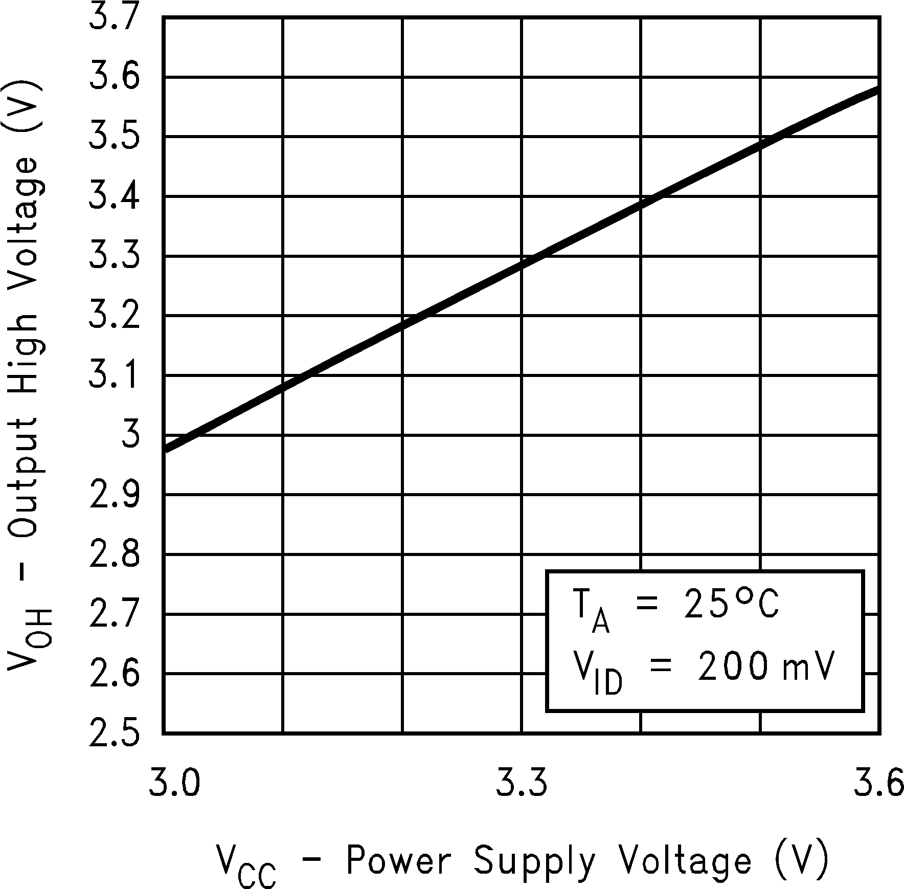 Figure 1. Output High Voltage
 vs Power Supply Voltage
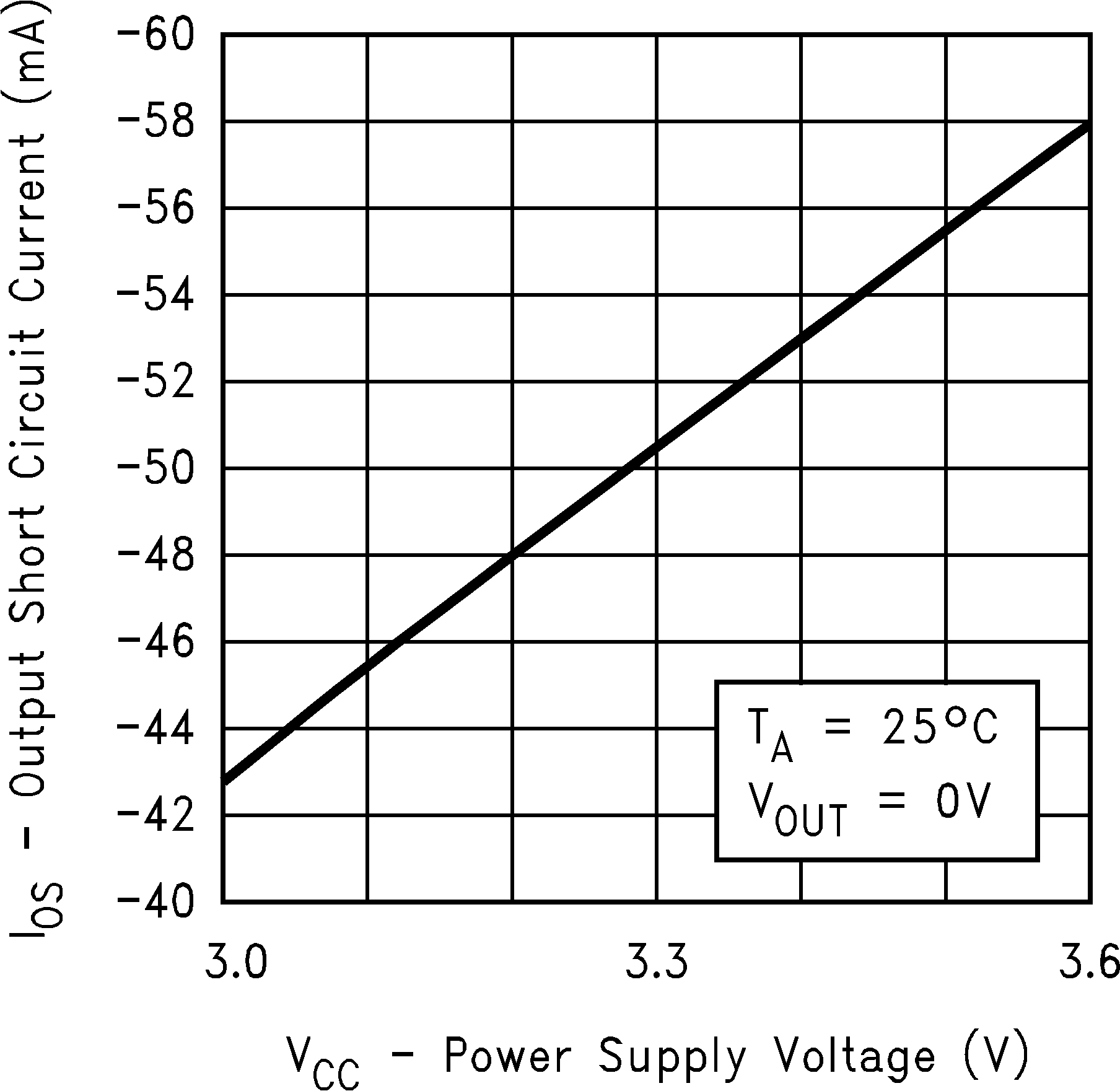 Figure 3. Output Short Circuit Current
 vs Power Supply Voltage
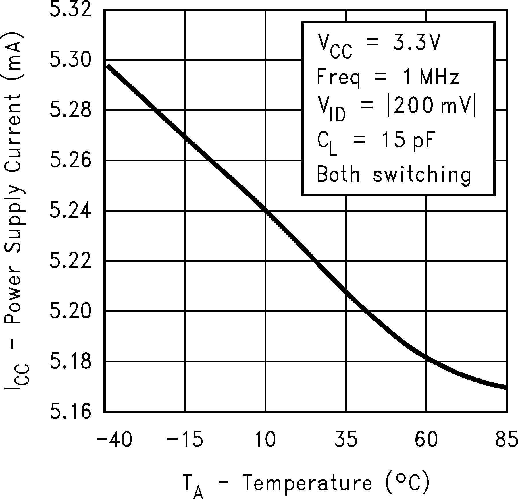 Figure 5. Power Supply Current
 vs Ambient Temperature
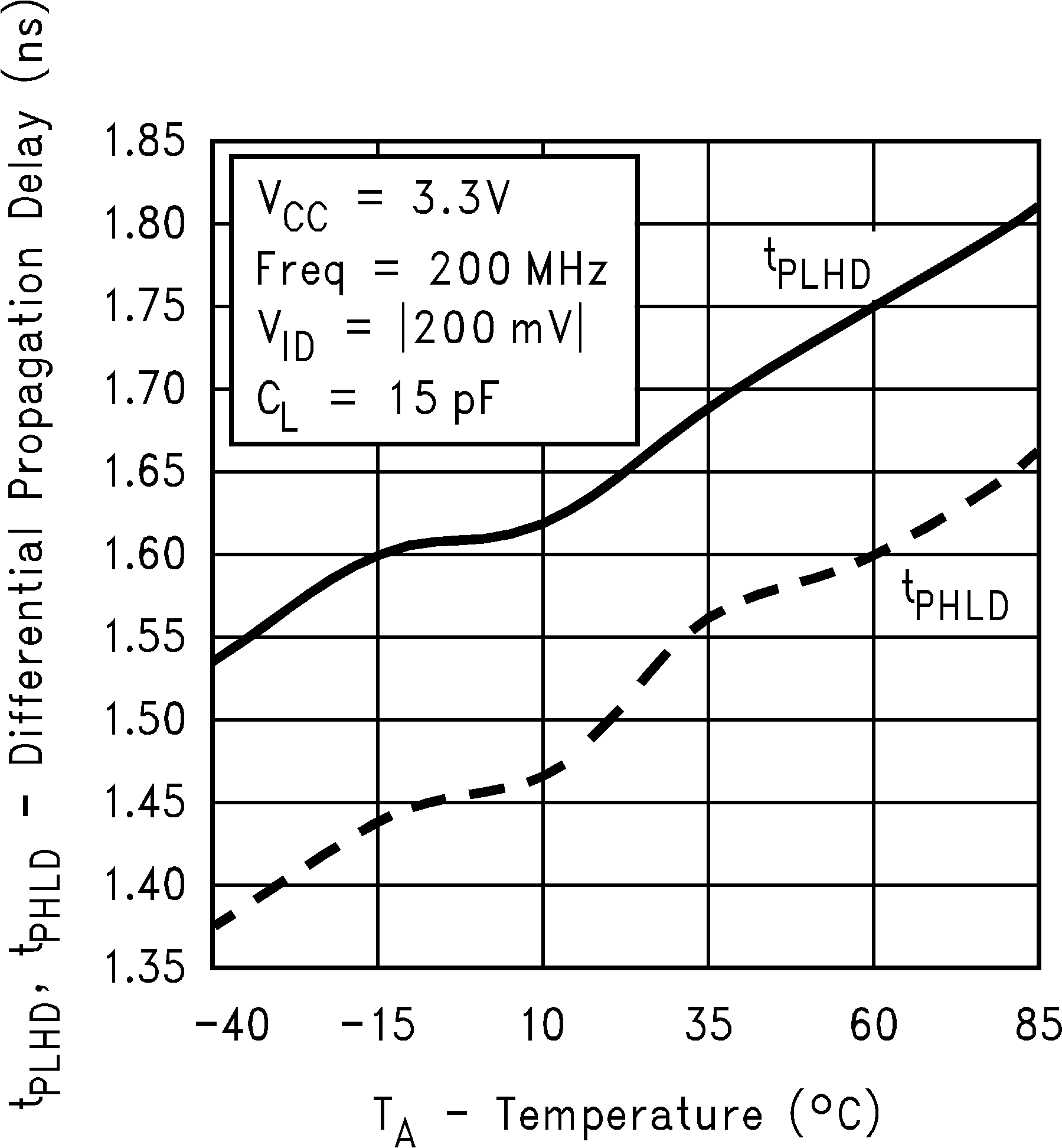 Figure 7. Differential Propagation Delay
 vs Ambient Temperature
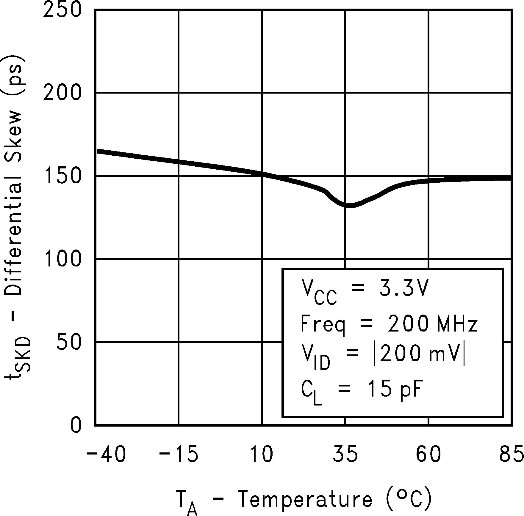 Figure 9. Differential Skew
 vs Ambient Temperature
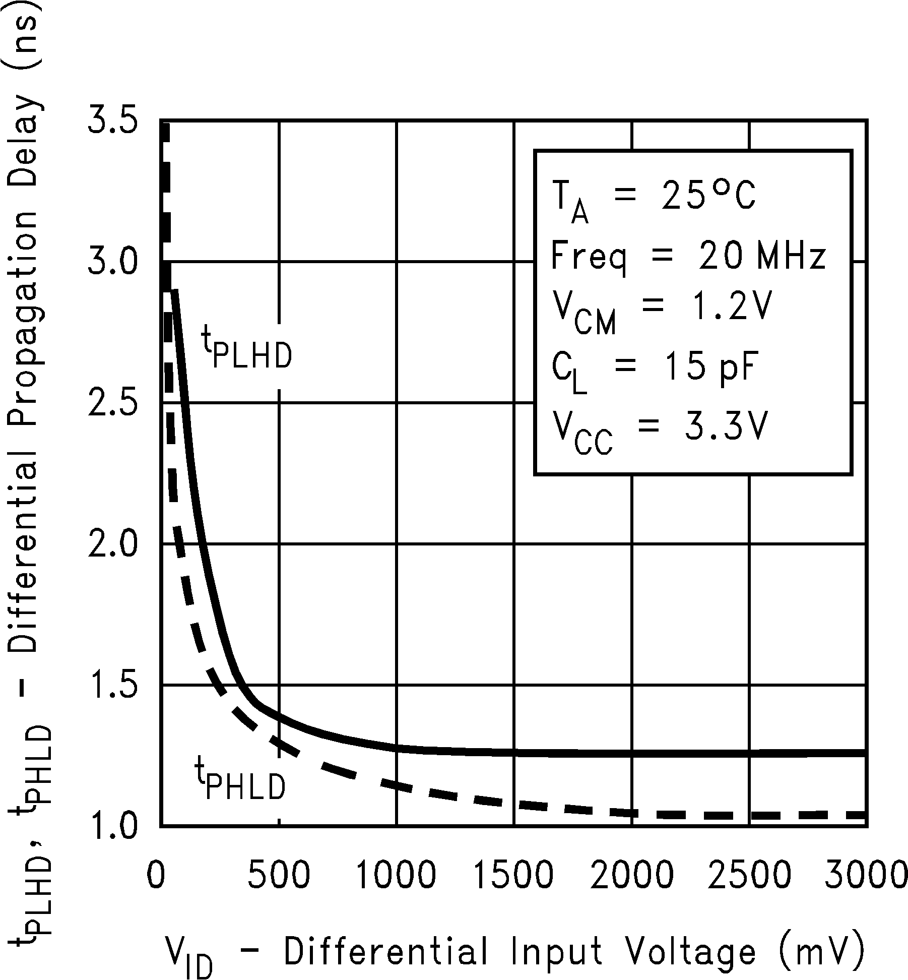 Figure 11. Differential Propagation Delay
 vs Differential Input Voltage
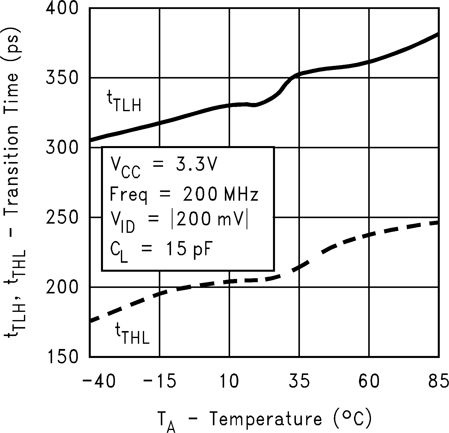 Figure 13. Transition Time
 vs Ambient Temperature
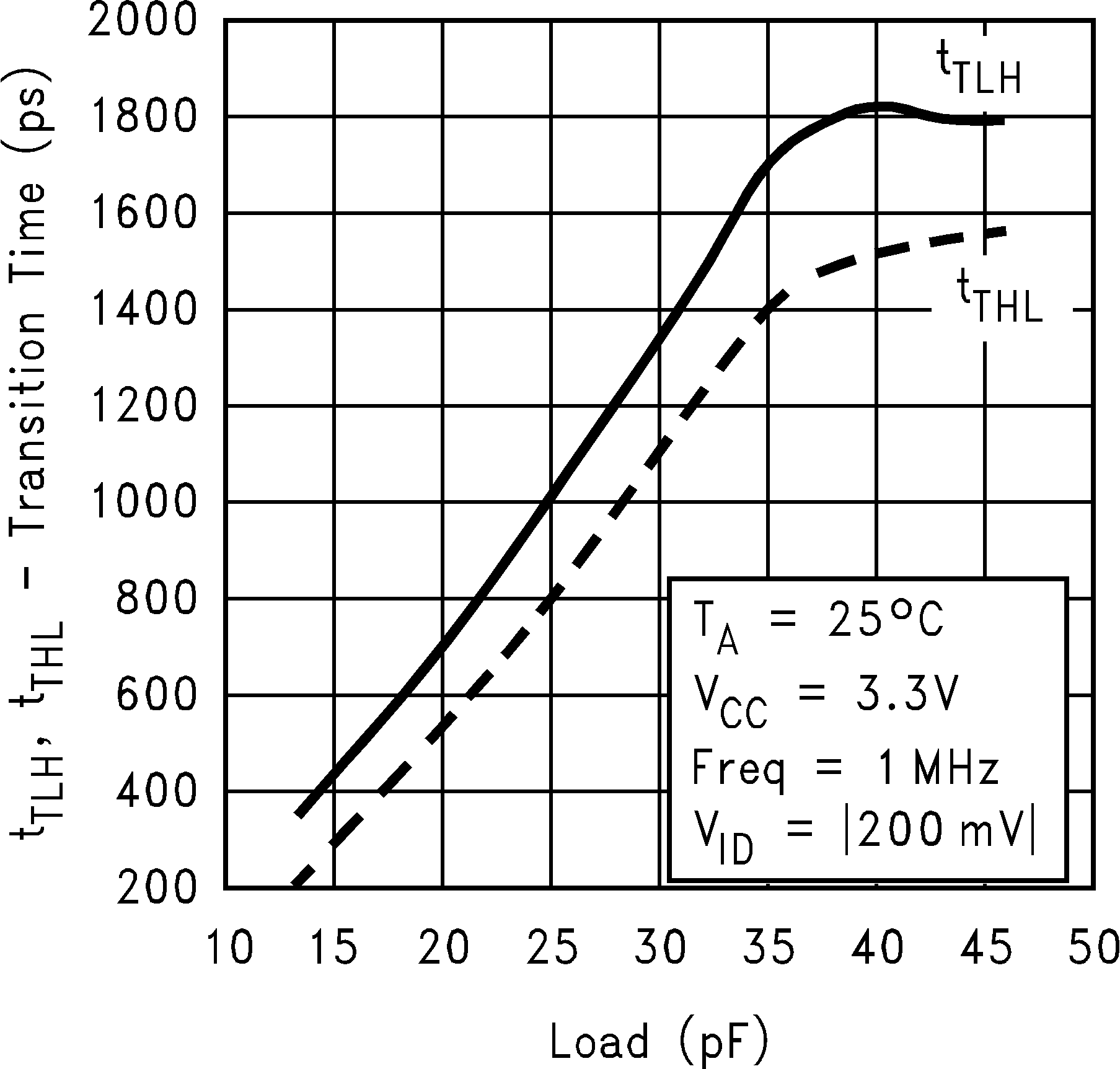 Figure 15. Transition Time
vs Load
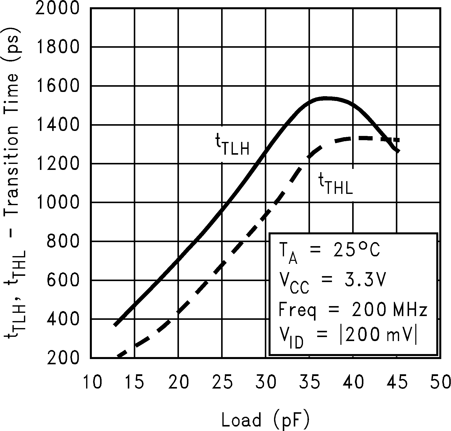 Figure 17. Transition Time
vs Load
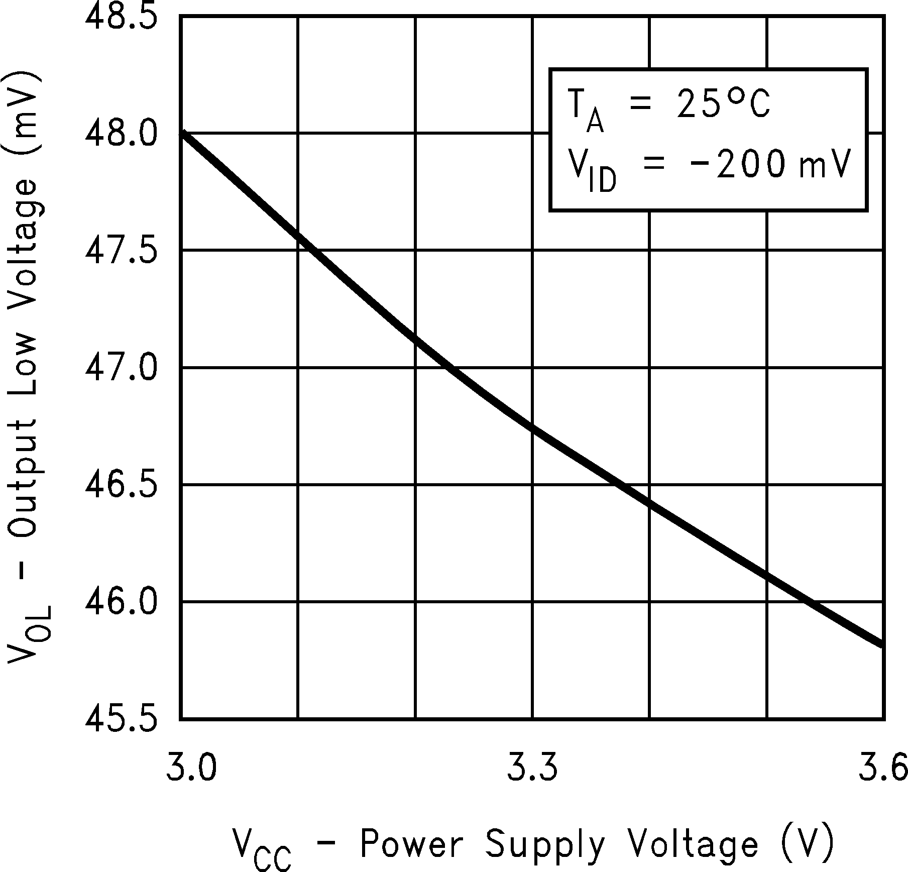 Figure 2. Output Low Voltage
 vs Power Supply Voltage
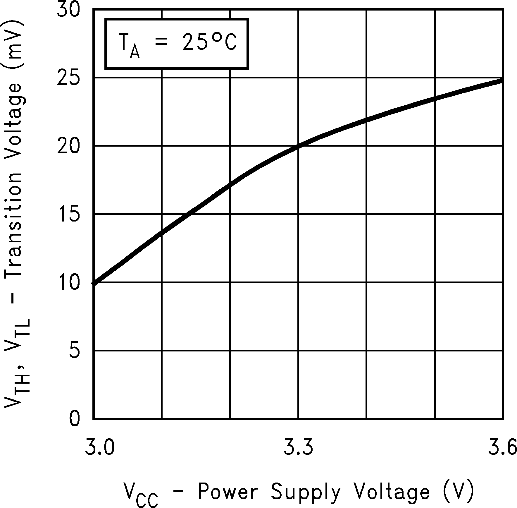 Figure 4. Differential Transition Voltage
 vs Power Supply Voltage
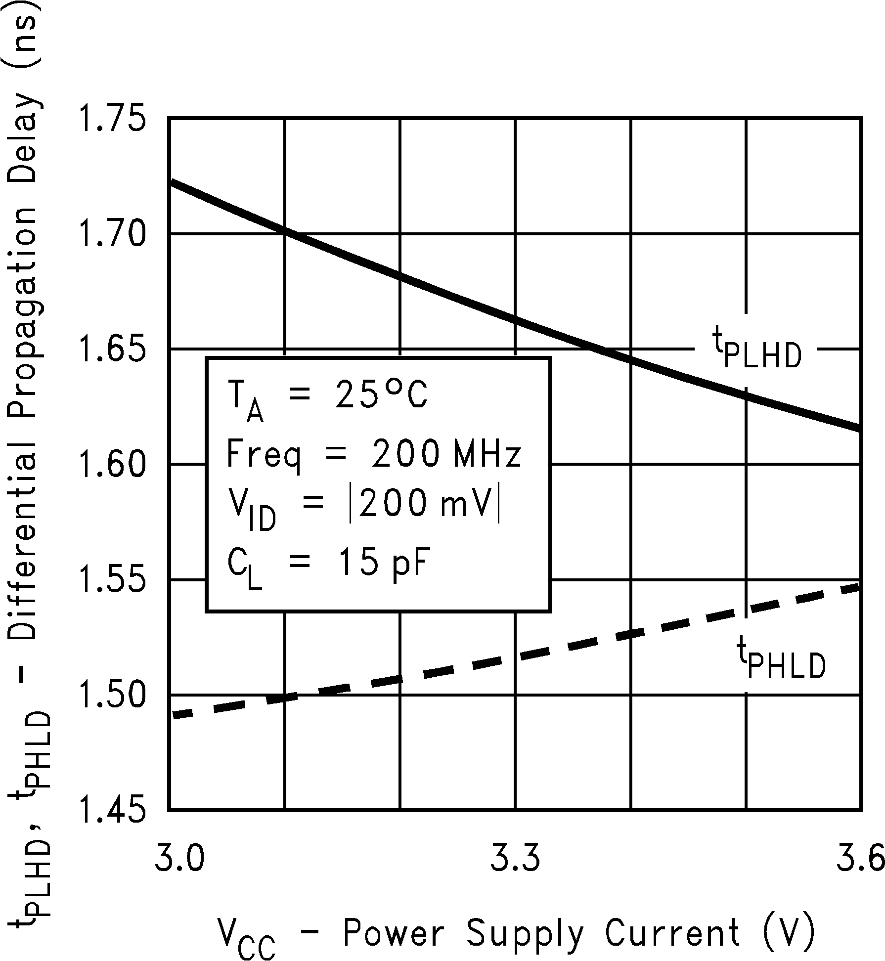 Figure 6. Differential Propagation Delay
 vs Power Supply Voltage
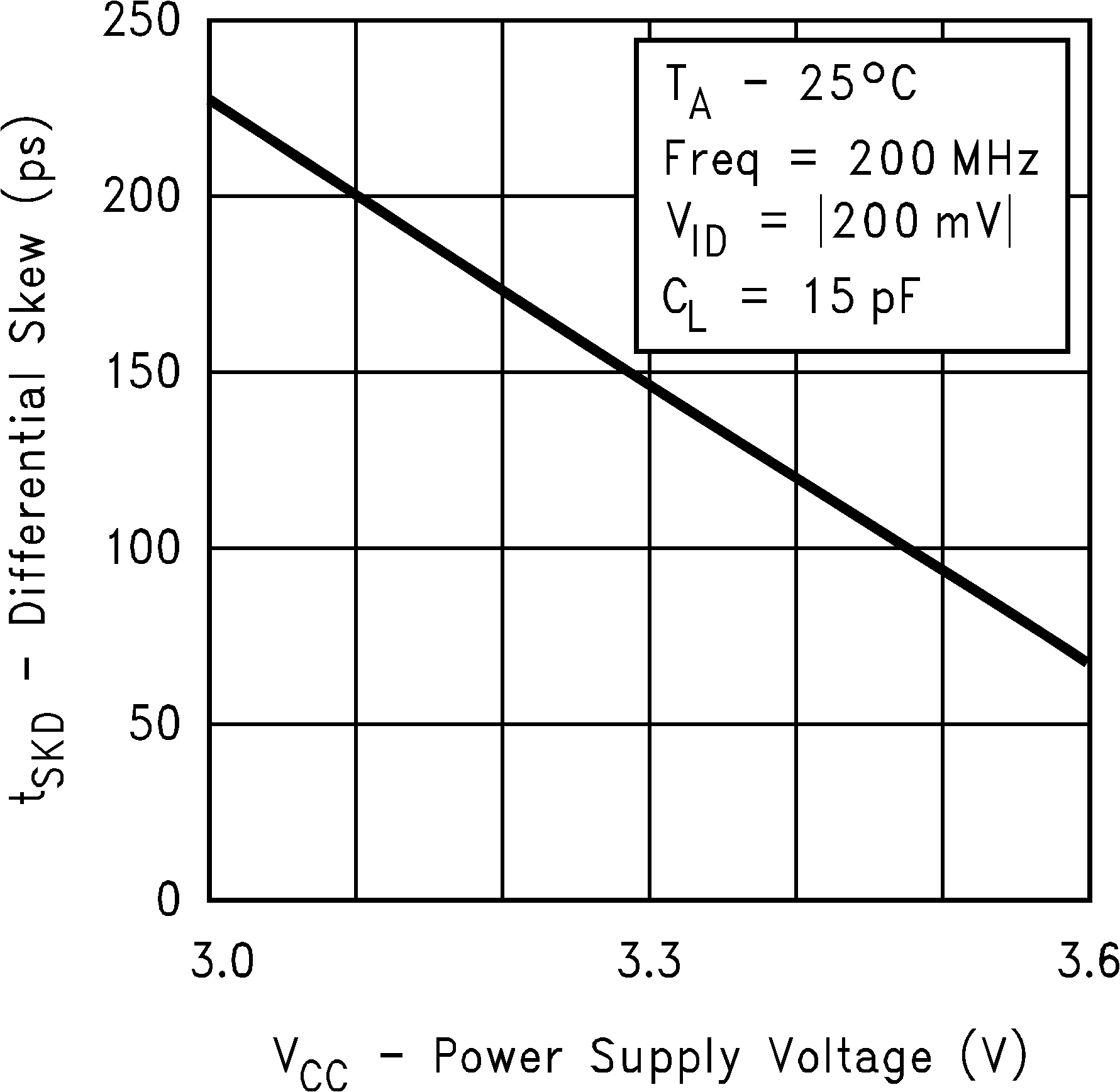 Figure 8. Differential Skew
 vs Power Supply Voltage
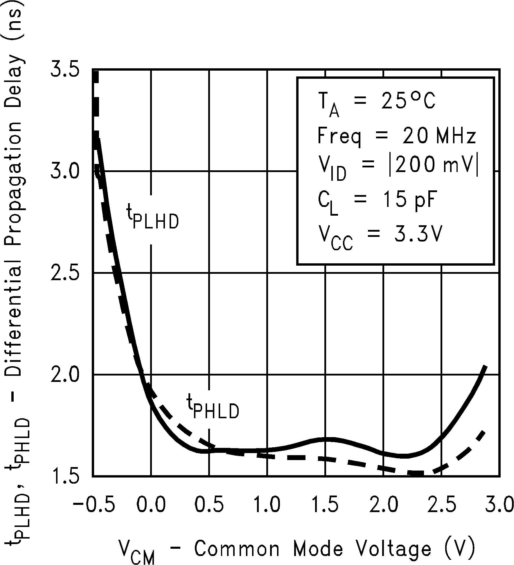 Figure 10. Differential Propagation Delay
 vs Common Mode Voltage
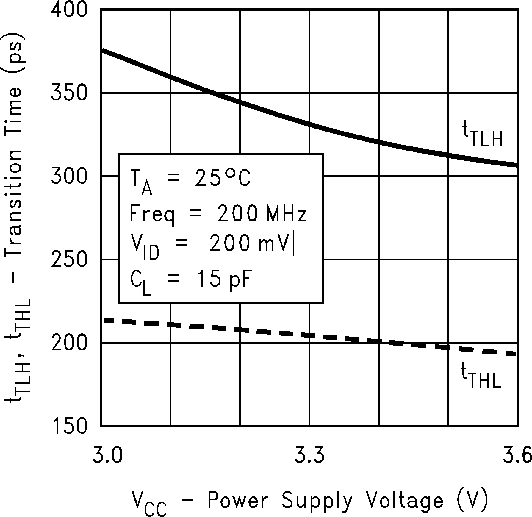 Figure 12. Transition Time
 vs Power Supply Voltage
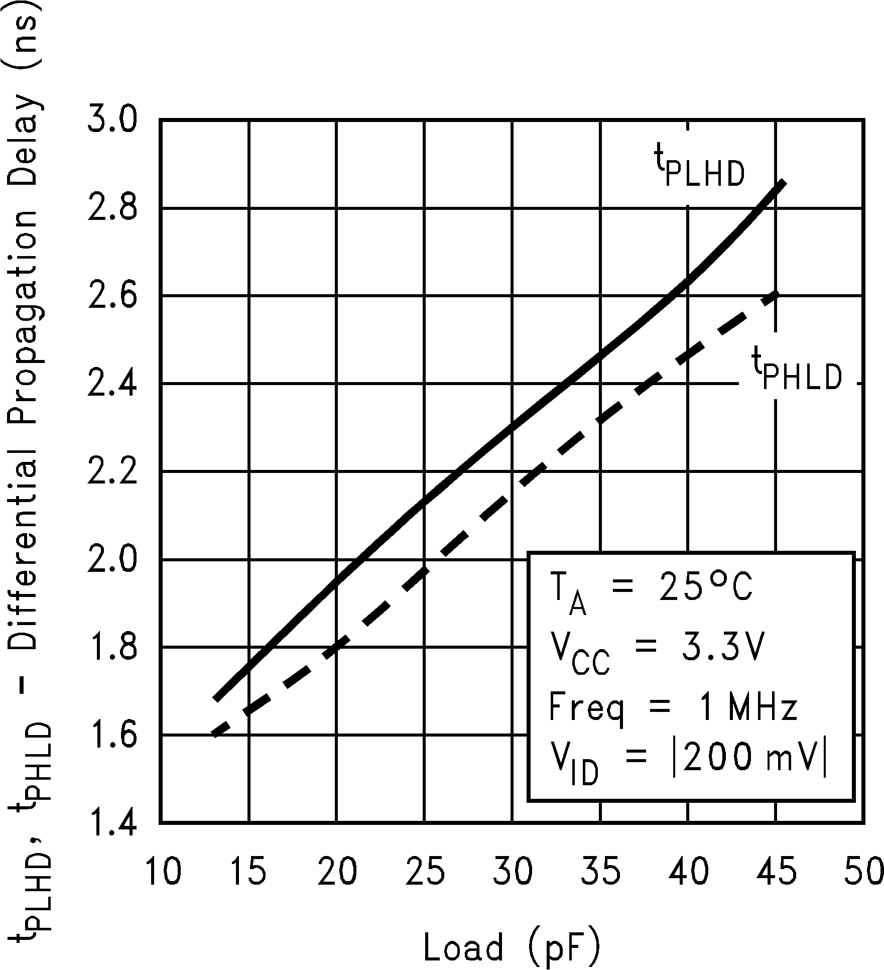 Figure 14. Differential Propagation Delay
vs Load
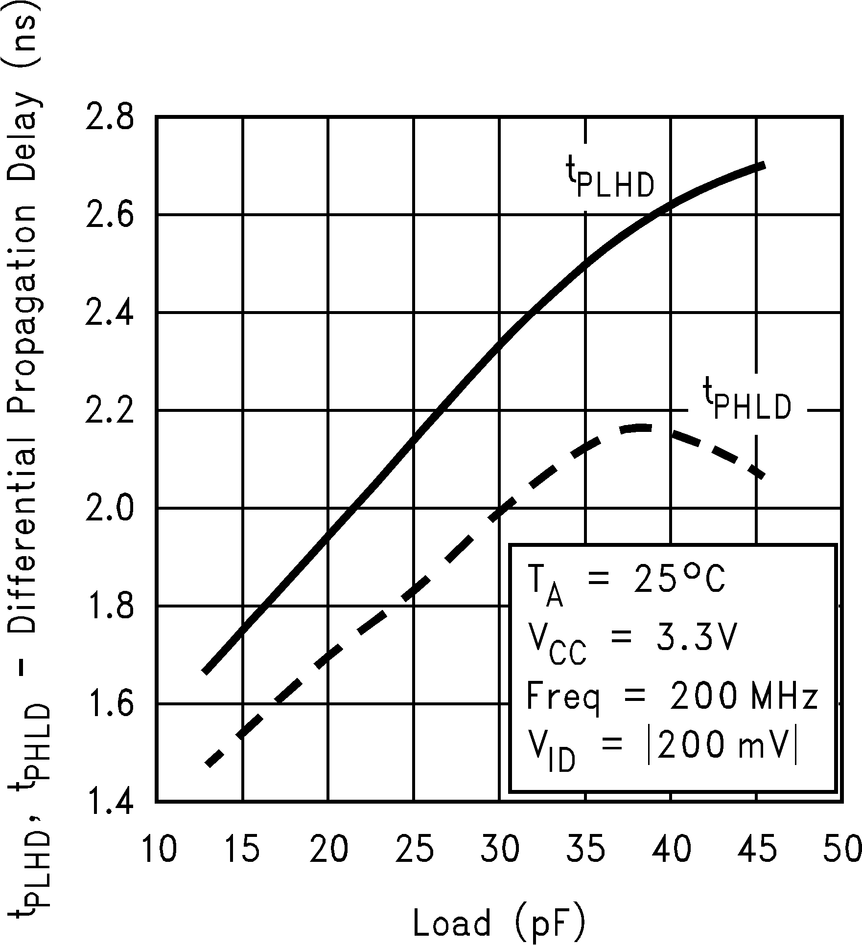 Figure 16. Differential Propagation Delay
vs Load