ZHCSJ91C September 2005 – July 2021 DS90LV011AH
PRODUCTION DATA
- 1 特性
- 2 应用
- 3 说明
- 4 Revision History
- 5 Pin Configuration and Functions
- 6 Specifications
- 7 Parameter Measurement Information
- 8 Detailed Description
- 9 Application and Implementation
- 10Power Supply Recommendations
- 11Layout
- 12Device and Documentation Support
- 13Mechanical, Packaging, and Orderable Information
9.2.2.2 Driver Bypass Capacitance
Bypass capacitors play a key role in power distribution circuitry. Specifically, they create low-impedance paths between power and ground. At low frequencies, a good digital power supply offers very low-impedance paths between its terminals. However, as higher frequency currents propagate through power traces, the source is quite often incapable of maintaining a low-impedance path to ground. Bypass capacitors are used to address this shortcoming. Usually, large bypass capacitors (10 μF to 1000 μF) at the board-level do a good job up into the kHz range. Due to their size and length of their leads, they tend to have large inductance values at the switching frequencies of modern digital circuitry. To solve this problem, one must resort to the use of smaller capacitors (nF to μF range) installed locally next to the integrated circuit.
Multilayer ceramic chip or surface-mount capacitors (size 0603 or 0805) minimize lead inductances of bypass capacitors in high-speed environments, because their lead inductance is about 1 nH. For comparison purposes, a typical capacitor with leads has a lead inductance around 5 nH.
The value of the bypass capacitors used locally with LVDS chips can be determined by Equation 1 and Equation 2 according to Johnson1 equations 8.18 to 8.21. A conservative rise time of 200 ps and a worst-case change in supply current of 1 A covers the whole range of LVDS devices offered by Texas Instruments. In this example, the maximum power supply noise tolerated is 200 mV. However, this figure varies depending on the noise budget available in the design. (1)
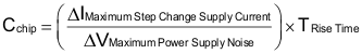
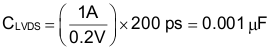
Figure 9-2 lowers lead inductance and covers intermediate frequencies between the board-level capacitor (>10 µF) and the value of capacitance found above (0.001 µF). TI recommends that the user place the smallest value of capacitance as close to the chip as possible.
 Figure 9-2 Recommended LVDS Bypass Capacitor Layout