ZHCSFI6E September 2015 – February 2017 DRV3205-Q1
PRODUCTION DATA.
10 Layout
10.1 Layout Guidelines
Use the following guidelines when designing a PCB for the DRV3205-Q1:
- In addition to the GND pins, the DRV3205-Q1 makes an electrical connection to GND through the PowerPAD. Always check that the PowerPAD has been properly soldered (see PowerPAD™ Thermally Enhanced Package [SLMA002]).
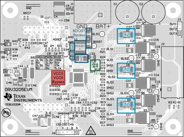
- The VS bypass capacitors should be placed close to the power supply terminals. See the VS box in Figure 19
- Place the VCC5 and VCC5 bypass capacitors close to the corresponding pins with a low impedance path to the ground plane pin (pin 16). See the VCC3 VCC5 bypass box in Figure 19.
- AGND should all be tied to the ground plane through a low impedance trace or copper fill.
- Add stitching vias to reduce the impedance of the GND path from the top to bottom side.
- Try to clear the space around and below the DRV3205-Q1 to allow for better heat spreading from the PowerPAD.
- Route the sense lines, IPx and INx, each with a unique trace, directly to either side of the sense resistor. See the SENSE box in Figure 19.
- Keep the BOOST components close to the device and current loops small. See the BOOST boxes in Figure 19.
- Place the current sense resistors close to the respective low-side FET. See the SENSE box in Figure 19.
- Place the GNDLS_B resistor close to the device pin. See the GNDLS_B box in Figure 19.
10.2 Layout Example
 Figure 19. Layout Schematic