ZHCSC07E December 2013 – March 2019 DLPC2607
PRODUCTION DATA.
- 1 特性
- 2 应用范围
- 3 说明
- 4 修订历史记录
- 5 Pin Configuration and Functions
-
6 Specifications
- 6.1 Absolute Maximum Ratings
- 6.2 ESD Ratings
- 6.3 Recommended Operating Conditions
- 6.4 Thermal Information
- 6.5 Typical Current and Power Dissipation
- 6.6 I/O Characteristics
- 6.7 Internal Pullup and Pulldown Characteristics
- 6.8 Parallel I/F Frame Timing Requirements
- 6.9 Parallel I/F General Timing Requirements
- 6.10 Parallel I/F Maximum Parallel Interface Horizontal Line Rate
- 6.11 BT.656 I/F General Timing Requirements
- 6.12 100- to 120-Hz Operational Limitations
- 6.13 Flash Interface Timing Requirements
- 6.14 DMD Interface Timing Requirements
- 6.15 mDDR Memory Interface Timing Requirements
- 7 Detailed Description
- 8 Application and Implementation
- 9 Power Supply Recommendations
-
10Layout
- 10.1
Layout Guidelines
- 10.1.1 Internal ASIC PLL Power
- 10.1.2 General Handling Guidelines for Unused CMOS-Type Pins
- 10.1.3 SPI Signal Routing
- 10.1.4 mDDR Memory and DMD Interface Considerations
- 10.1.5 PCB Design
- 10.1.6 General PCB Routing (Applies to All Corresponding PCB Signals)
- 10.1.7 Maximum, Pin-to-Pin, PCB Interconnects Etch Lengths
- 10.1.8 I/F Specific PCB Routing
- 10.1.9 Number of Layer Changes
- 10.1.10 Stubs
- 10.1.11 Termination Requirements:
- 10.2 Layout Example
- 10.1
Layout Guidelines
- 11器件和文档支持
- 12机械、封装和可订购信息
请参考 PDF 数据表获取器件具体的封装图。
机械数据 (封装 | 引脚)
- ZVB|176
散热焊盘机械数据 (封装 | 引脚)
10.1.1 Internal ASIC PLL Power
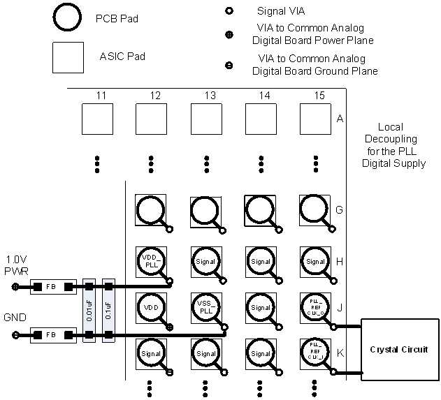
TI recommends the following guidelines to achieve desired ASIC performance relative to the internal PLL. The DLPC2607 device contains one internal PLL, which has a dedicated analog supply (VDD_PLL and VSS_PLL). Isolate VDD_PLL power and VSS_PLL ground pins using an RC-filter consisting of two 50-Ω series ferrites and two shunt capacitors (to widen the spectrum of noise absorption). TI recommends one 0.1-µF capacitor and that the other is a 0.01-µF capacitor. Place all four components as close to the ASIC as possible; it is especially important to keep the leads of the high-frequency capacitors as short as possible. Note that the user should connect both capacitors across VDD_PLL and VSS_PLL on the ASIC side of the ferrites.
The PCB layout is critical to PLL performance. The ground and power domains are analog signals, and should be treated as such to achieve minimum noise. Therefore, VDD_PLL must be a single trace from the DLPC2607 device to both capacitors, and then through the series ferrites to the power source. Ensure that the power and ground traces are as short as possible, parallel to each other, and as close as possible to each other.
 Figure 15. PLL Filter Layout